


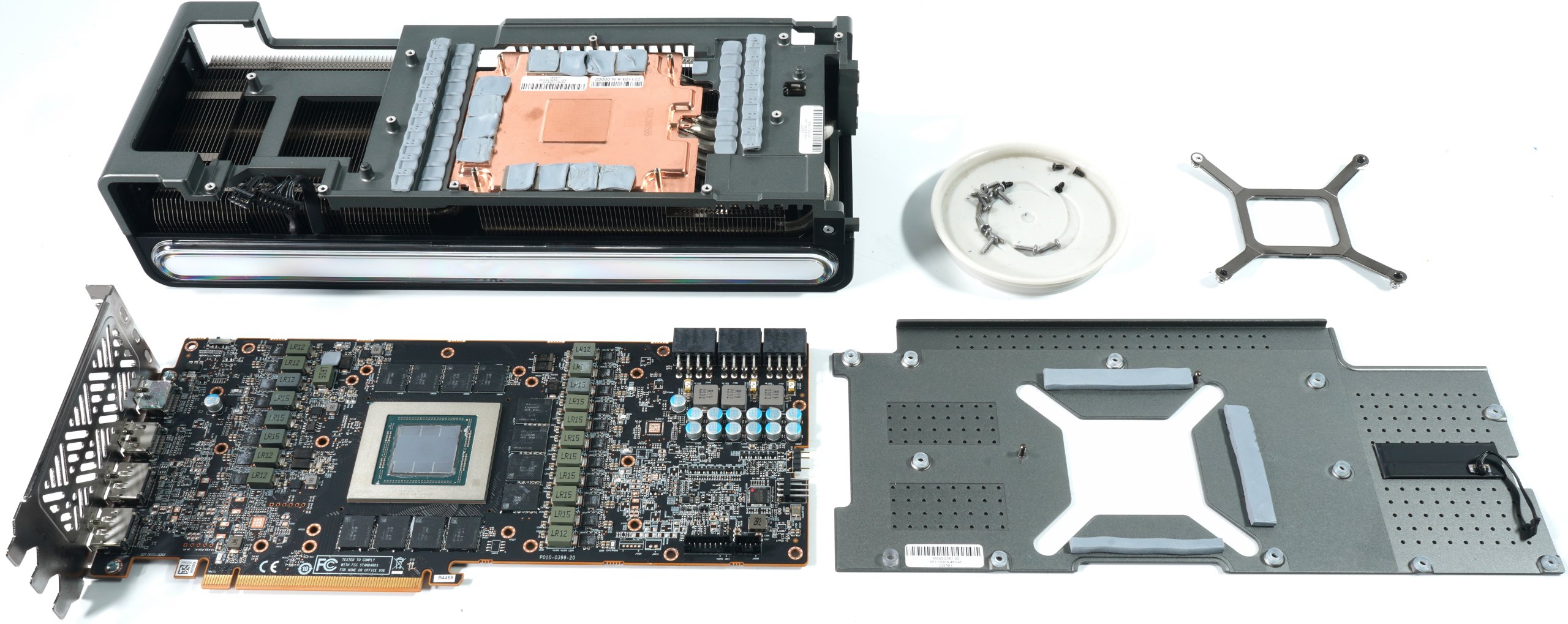
Now let’s get to the disassembly of the card and the exciting details inside. Taking it apart is relatively easy if you carefully loosen all the connectors. All screws are located on the back of the backplate or on the slot bracket. The clamping cross has two seals.
PCB layout and components
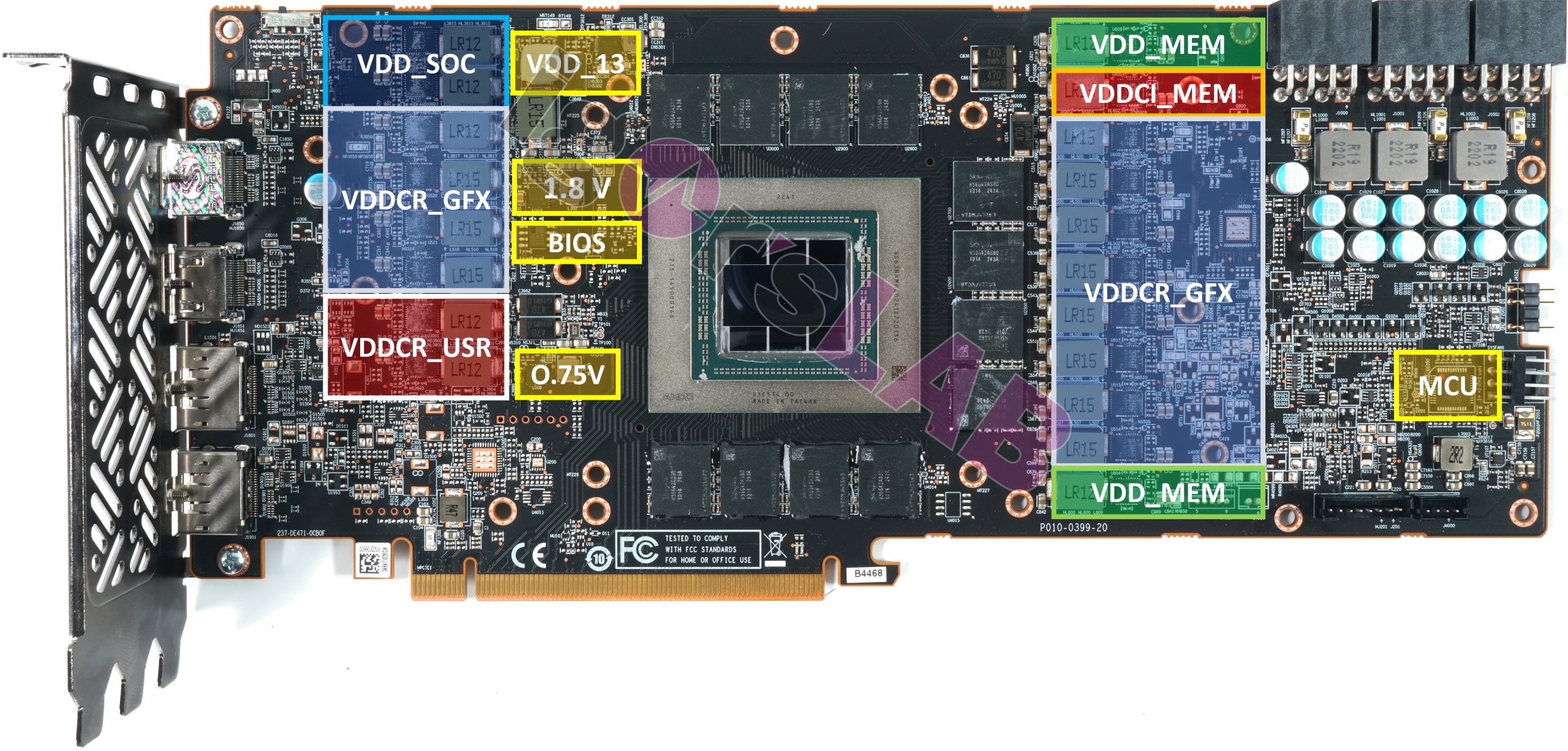
In principle, the PCB is very similar to AMD’s reference card. Here we also find VDDCR_GFX and they also use 12 real phases, each driving a single voltage regulator. However, VDD_SoC shrinks to two instead of three phases and one voltage regulator per phase. VDDCR_USR is added with two phases and thus also two additional voltage regulators. This is supplemented with three phases or three voltage regulators for VDD_MEM and an em single buck converter for VDDCI_MEM.
The generation of VDDCI_MEM is not a big item in terms of performance, but it is still enormously important. It serves the GPU-internal level transition between the GPU and the memory signal, something like the voltage between the memory and the GPU core on the I/O bus. In addition, one still generates a constant source for 0.75 volts. The majority of these very similar voltage converters are located on the front of the board. In addition, there is also a 1.8V source (TTL, GPU GPIO), VDD_13 (Aux) and an ultra-low dropout chip generates the very low voltage for the PLL area (VPP).
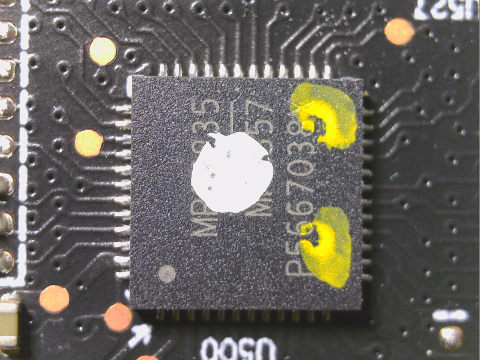
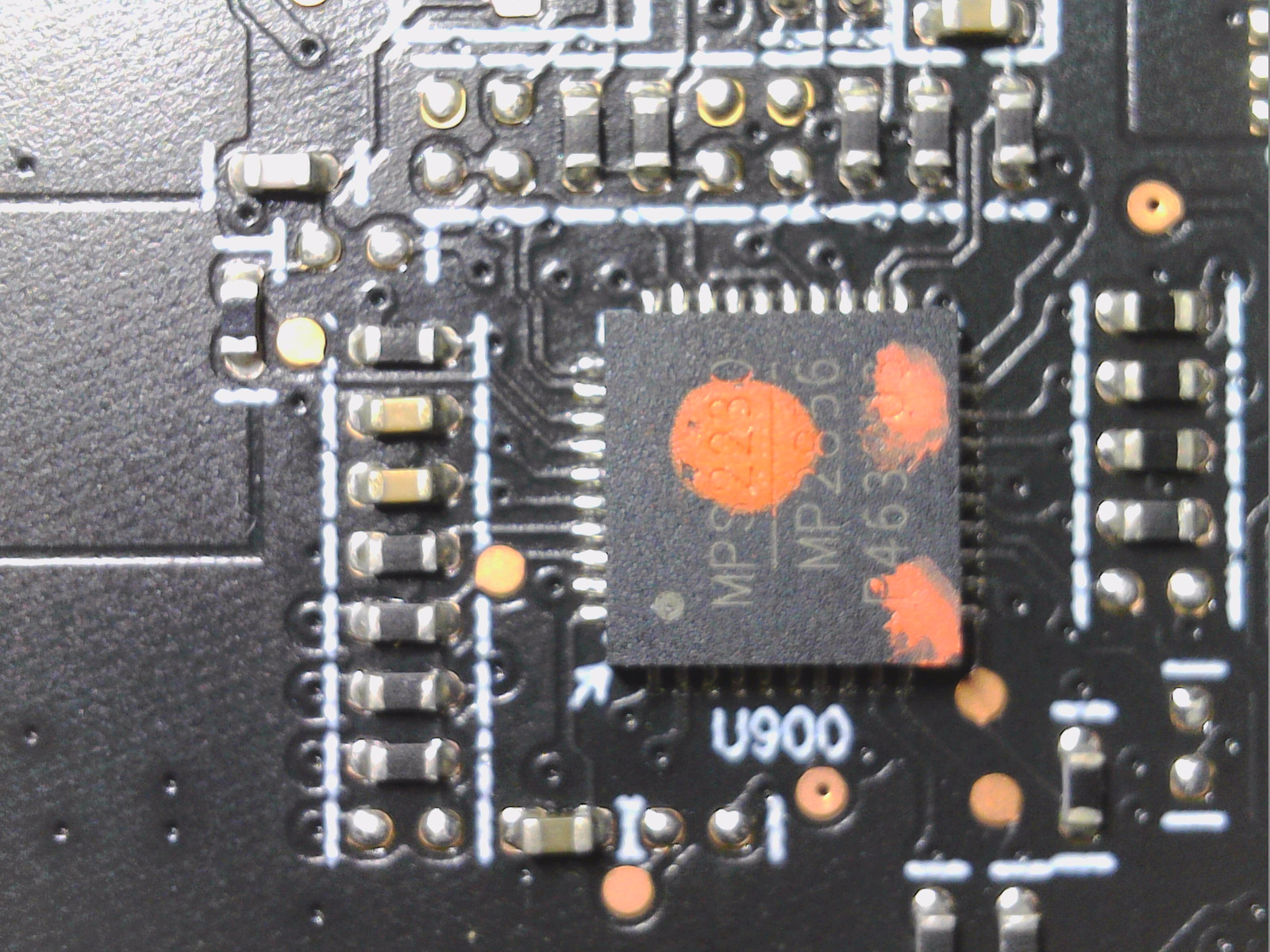
On the back (pictured below), two PWM controllers sit in the upper left third of the board for generating the main phases (red and blue), with another on the upper right (green). AMD relies on Monolith’s top products this time, just like NVIDIA did for the reference cards. The first rail of the MP2857 (blue) is used for the 12 phases of the VDDCR_GFX, the second rail for the generation of the VDD_MEM. It is a digital, multiphase, dual-rail controller that primarily provides power to PWM VID cores and is also compatible with the AVSBus interface.
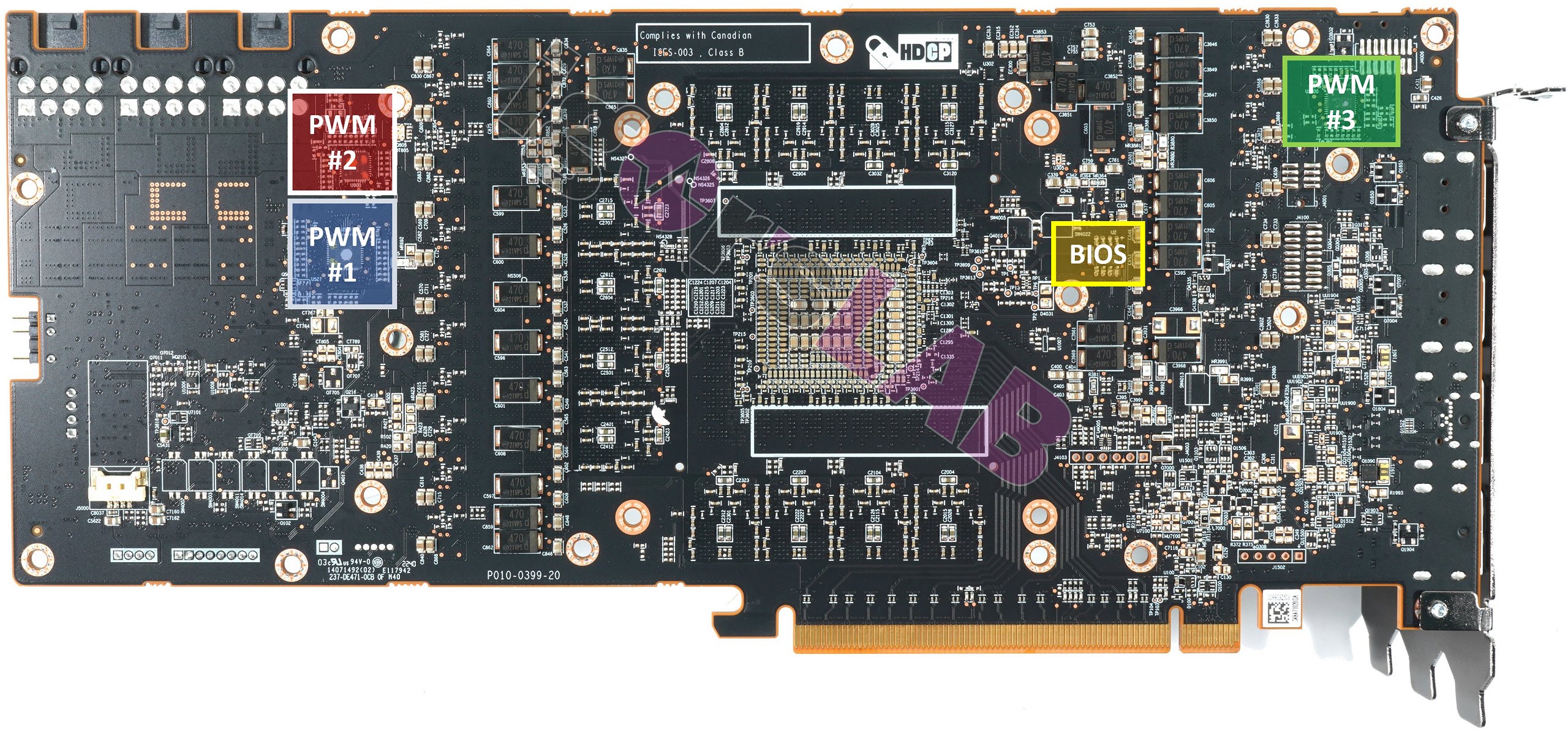
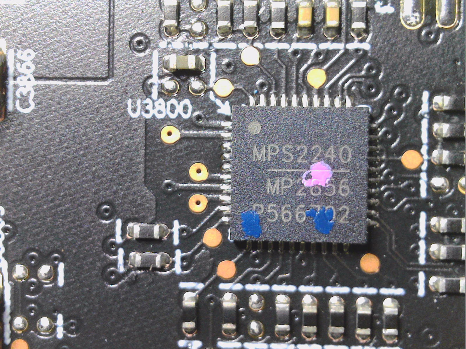
The MP2857 can (and should) also work with Monolith’s Intelli-Phase products to complete the multi-phase voltage regulator (VR) solution with a minimum of external components. The two slightly smaller MP2856 (red) and MP2240 (green), which are unfortunately also not publicly available in terms of data, are then responsible for VDDCI, VDD_SoC and VDDCR_USR, depending on the side.
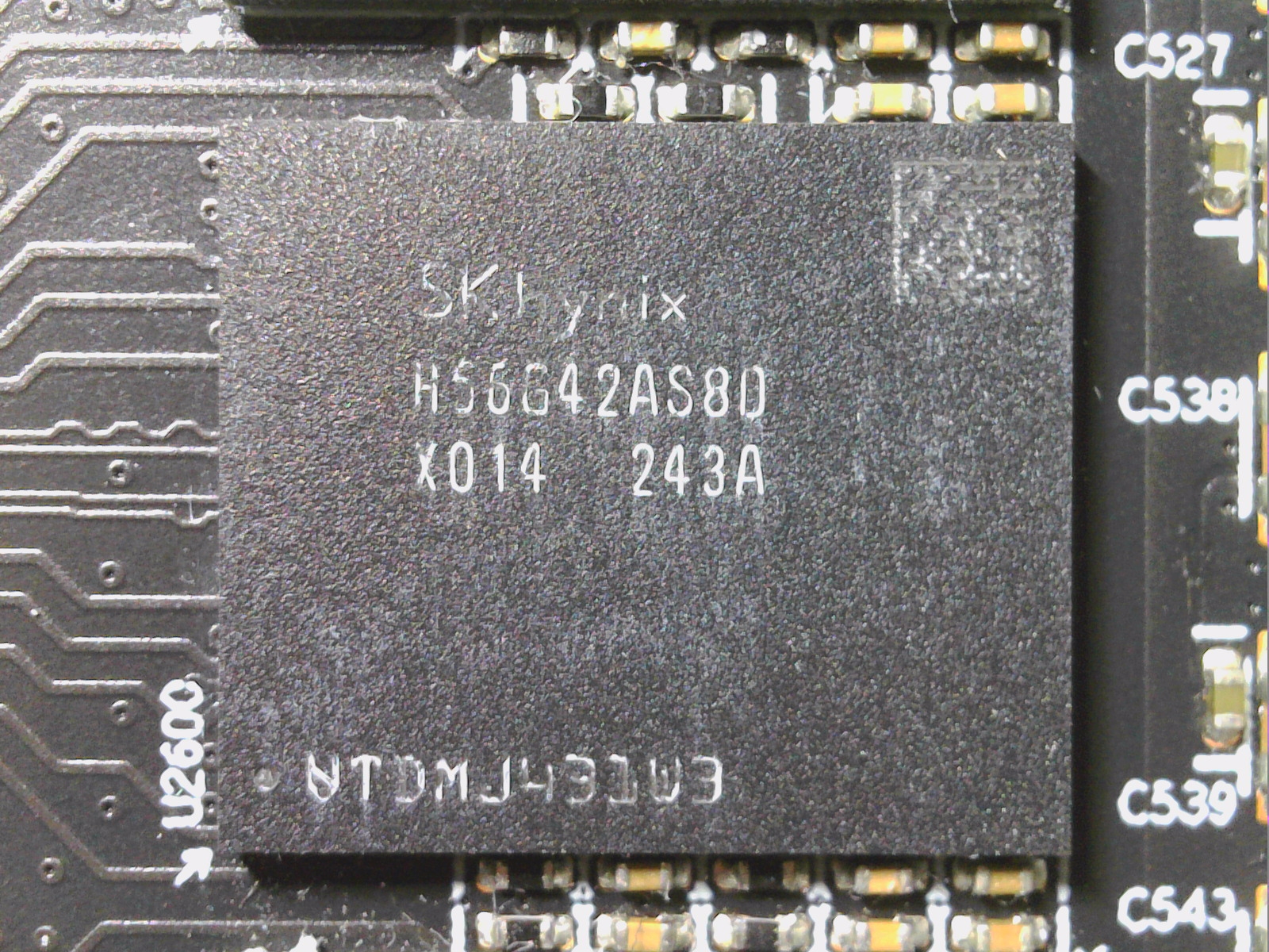
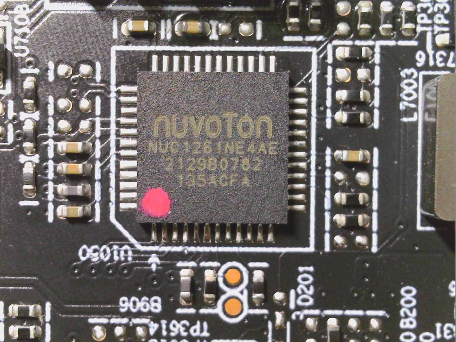
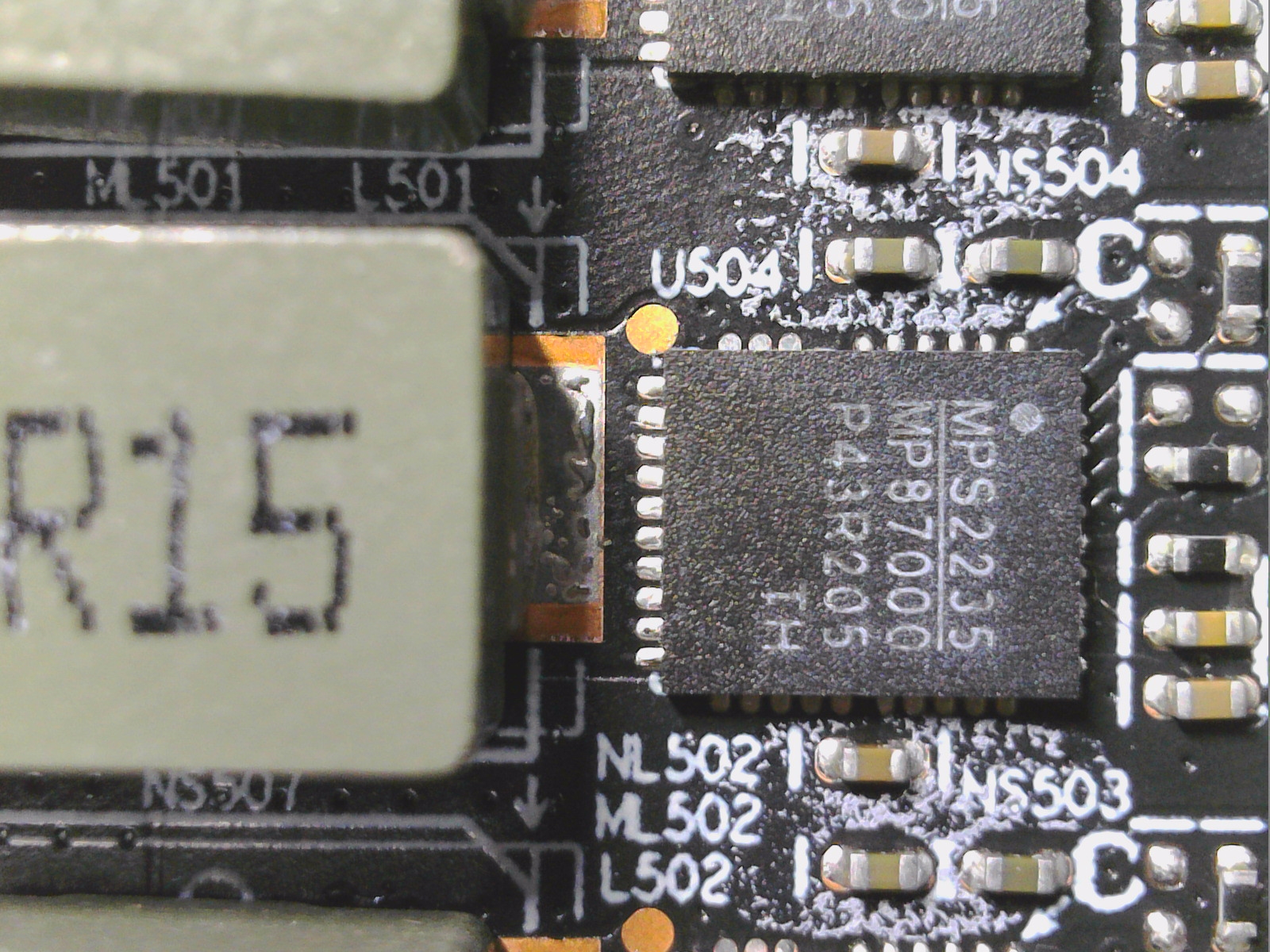
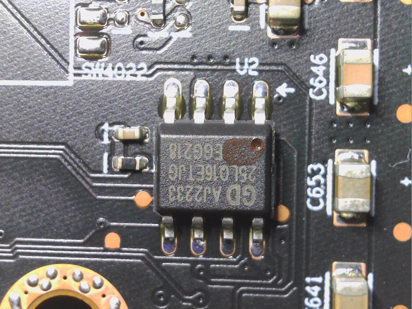
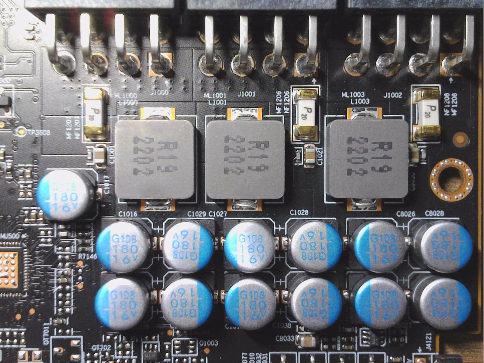
All power stages used, including those for the memory, are also products from Monolith. The MP87000 is also quite new and not freely documented, but it should be a very powerful Monolith half-bridge. The integration of drivers and MOSFETs (DrMOS) results in high efficiency due to optimal dead time and a reduction in parasitic inductance. This small, 5 mm x 6 mm LGA device is a perfect match for the PWM controllers used by Monolith. An MCU for all the control tasks is integrated this time (front side) and of course we have the 12 RAM modules from SK hynix with the 20 Gbps.

- 1 - Introduction, technical data and technology
- 2 - Teardown: PCB and components
- 3 - Teardown: Cooler and disassembly tips
- 4 - Gaming Performance Full-HD (1920 x 1080)
- 5 - Gaming Performance WQHD (2560 x 1440)
- 6 - Summe Gaming-Performance Ultra-HD (3840 x 2160)
- 7 - Power consumption and load balacing
- 8 - Load peaks, capping and power supply recommendation
- 9 - Temperatures, clock rates and infrared analysis
- 10 - Fan curves and volume
- 11 - Summary and conclusion


200 Antworten
Kommentar
Lade neue Kommentare
Mitglied
Veteran
Urgestein
Mitglied
Veteran
Urgestein
Urgestein
1
Veteran
Urgestein
1
Urgestein
Veteran
Urgestein
Urgestein
Urgestein
Mitglied
Urgestein
Alle Kommentare lesen unter igor´sLAB Community →