


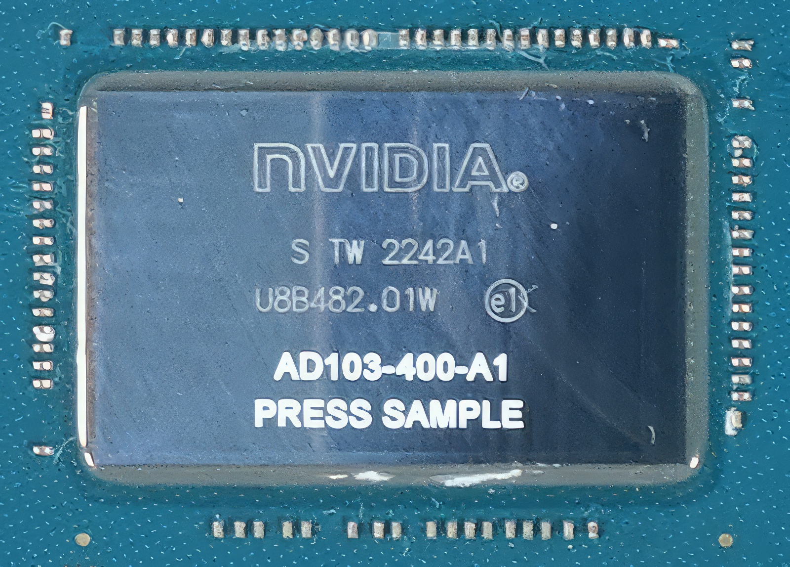
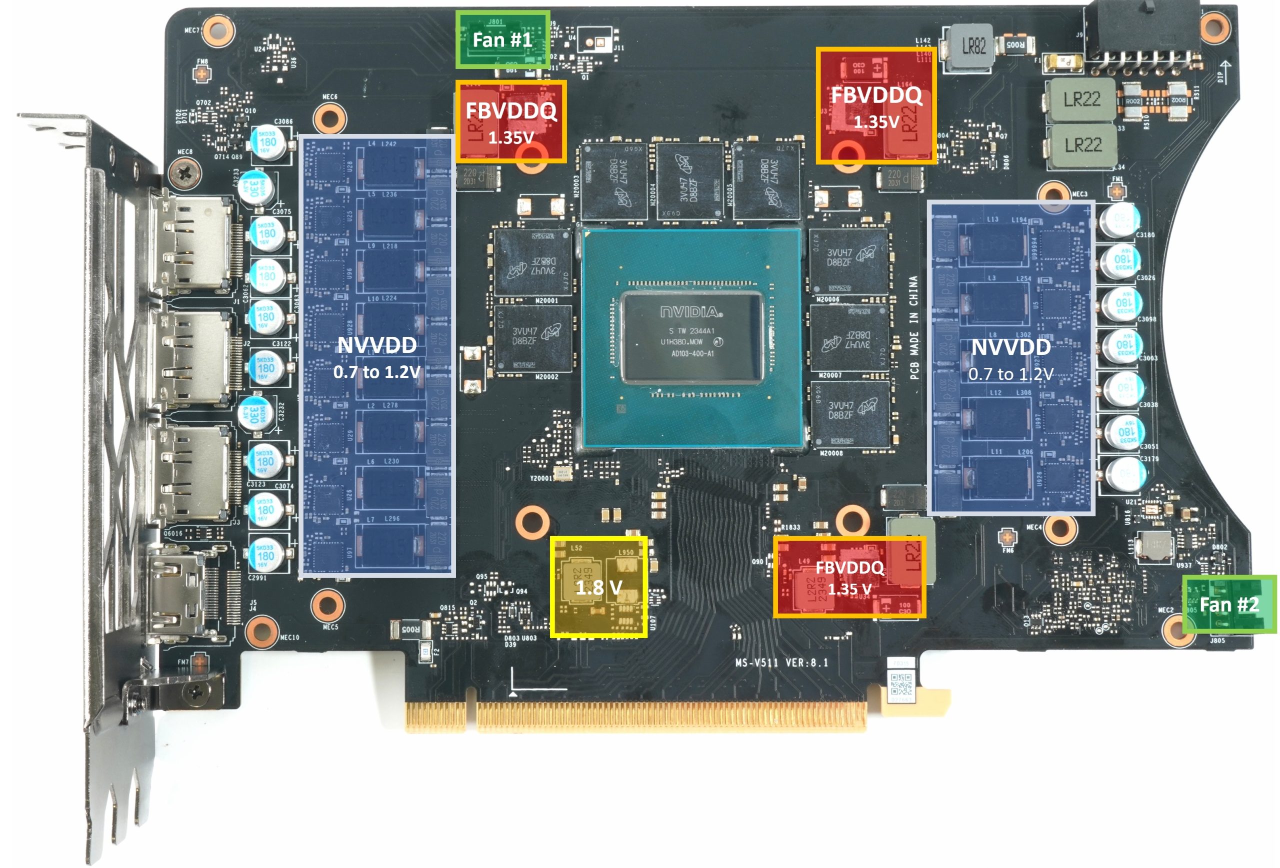
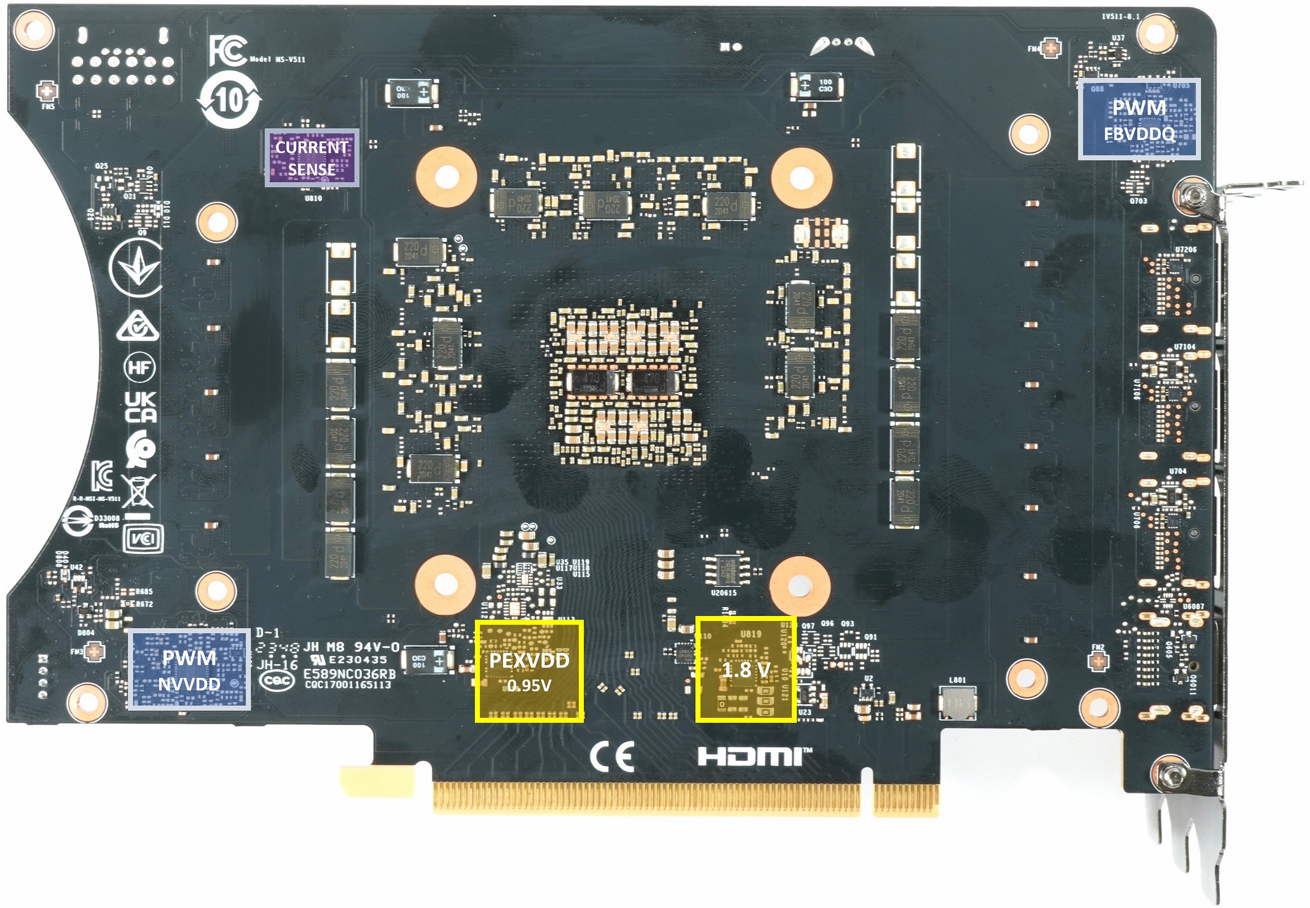
Teardown: PCB layout and components of the NVIDIA RTX 4080 Super Founders Edition 16GB
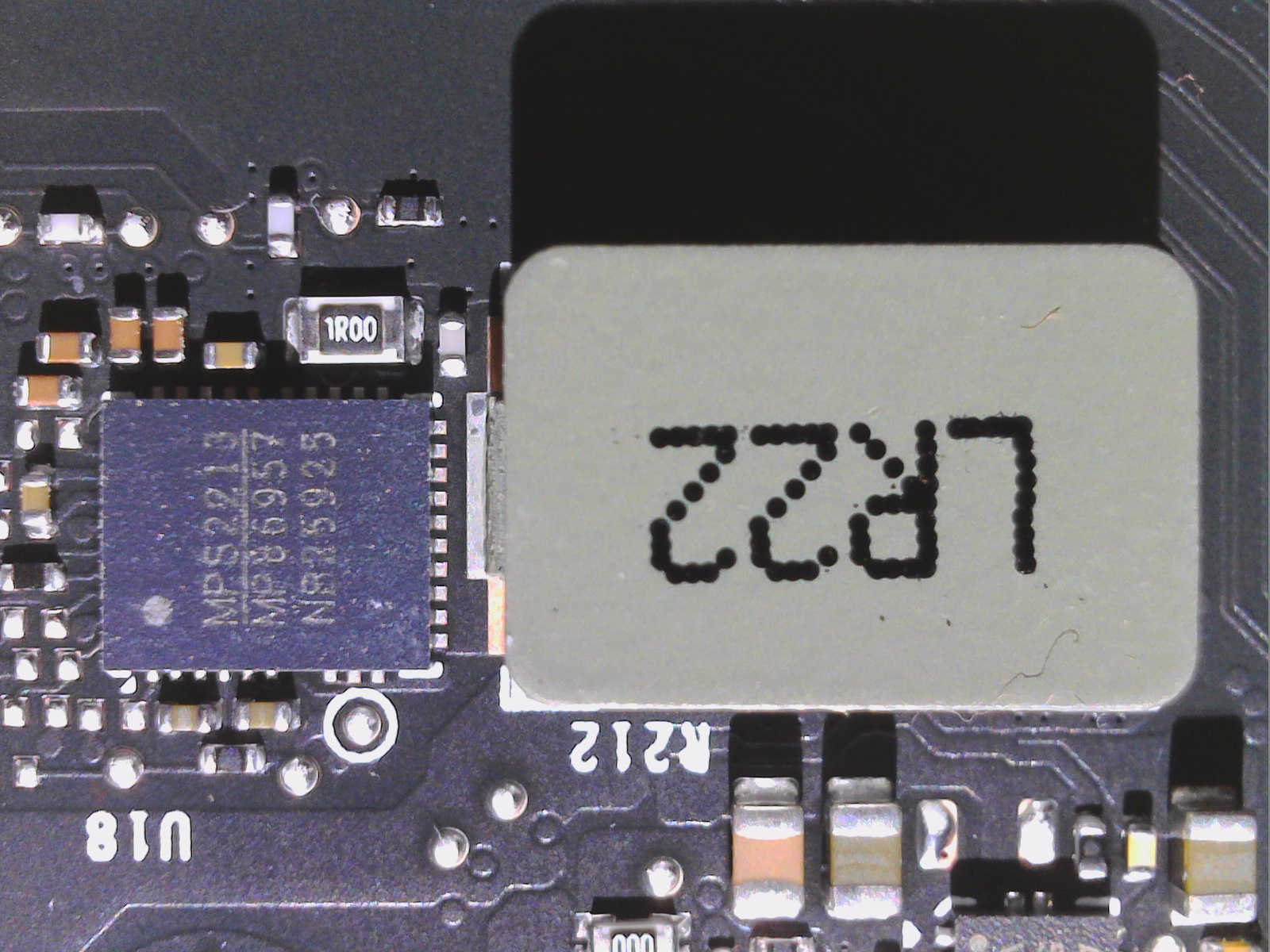
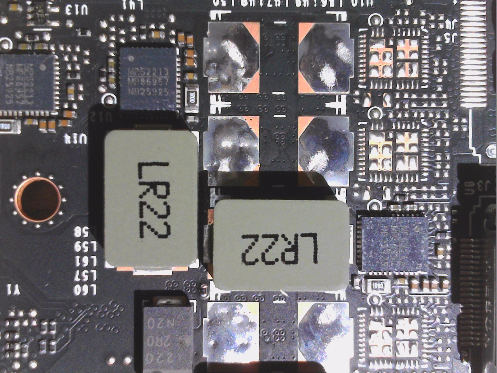
Let’s start with the PCB itself. NVVDD is the most important voltage and MSVDD has also been buried for good this time. This also results in the voltage converter design with a total of 10 phases and the resulting 10 control circuits for NVVDD (only one per phase). The GeForce RTX 4090 FE still relied on 10 phases and a total of 20 voltage converters, i.e. two per phase in parallel. It makes perfect sense to rely on a solid single circuit instead of doubling, because with the now higher switching frequencies, twice the number of phases would only be a hindrance due to the inertia of the coils and caps. Cheaper cards will probably go back to 8 phases, because the better PWM controllers and also the DrMOS cost money. But on the FE, NVIDIA has gone the extra mile and installed only the finest components.
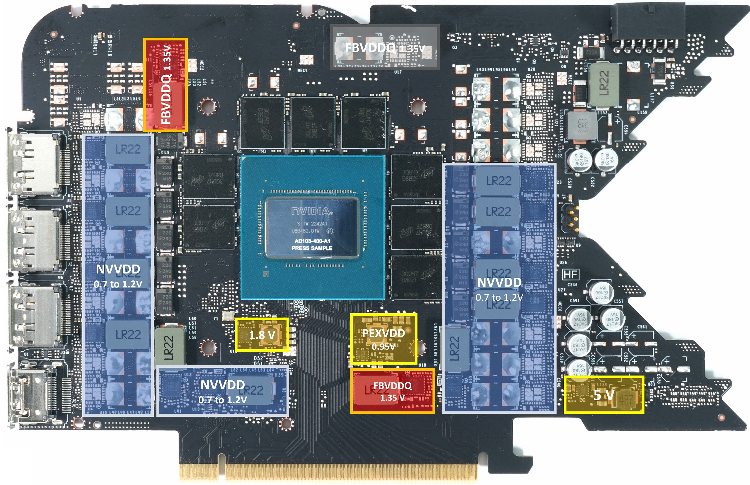
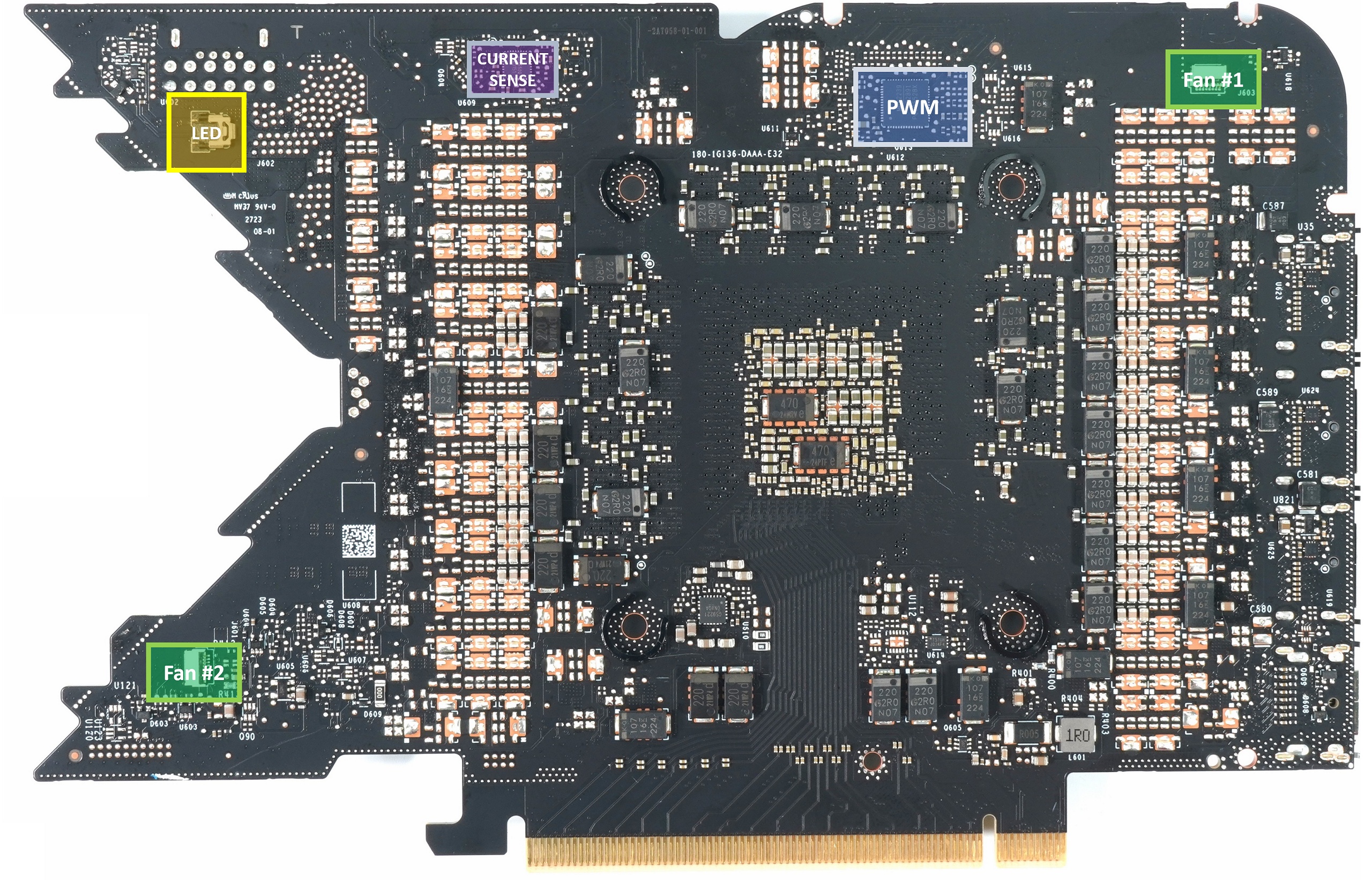
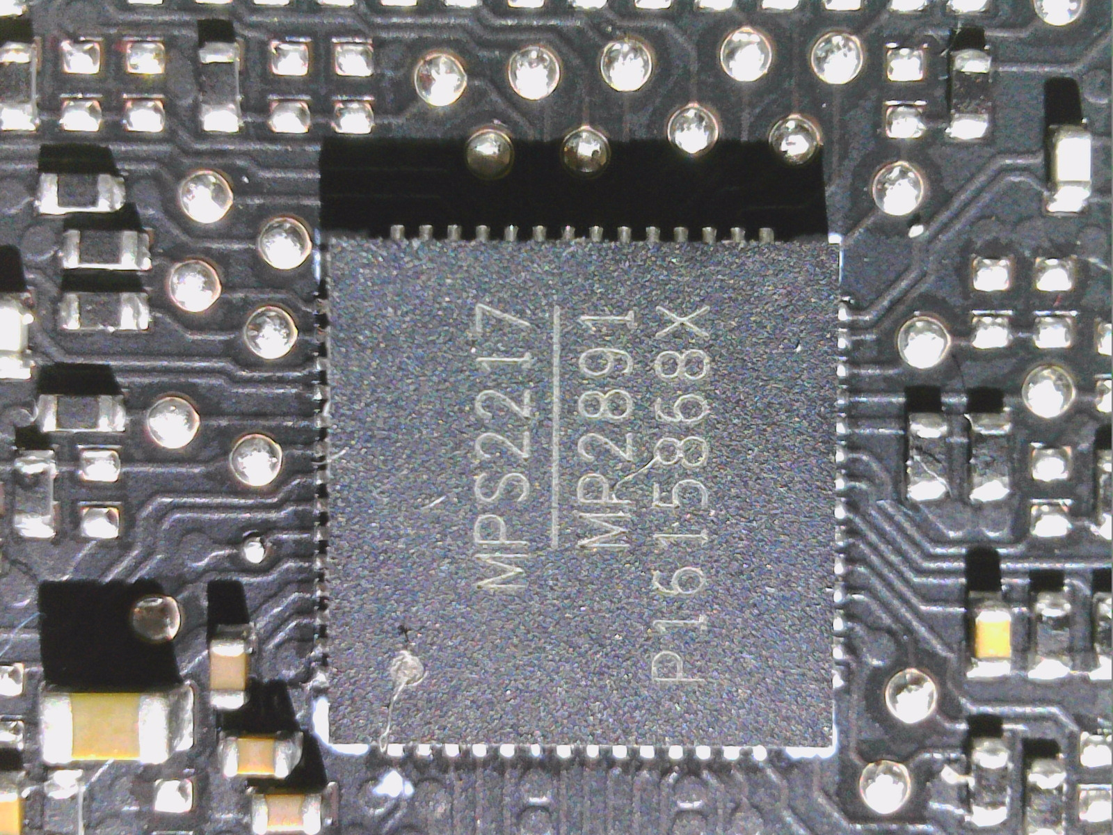
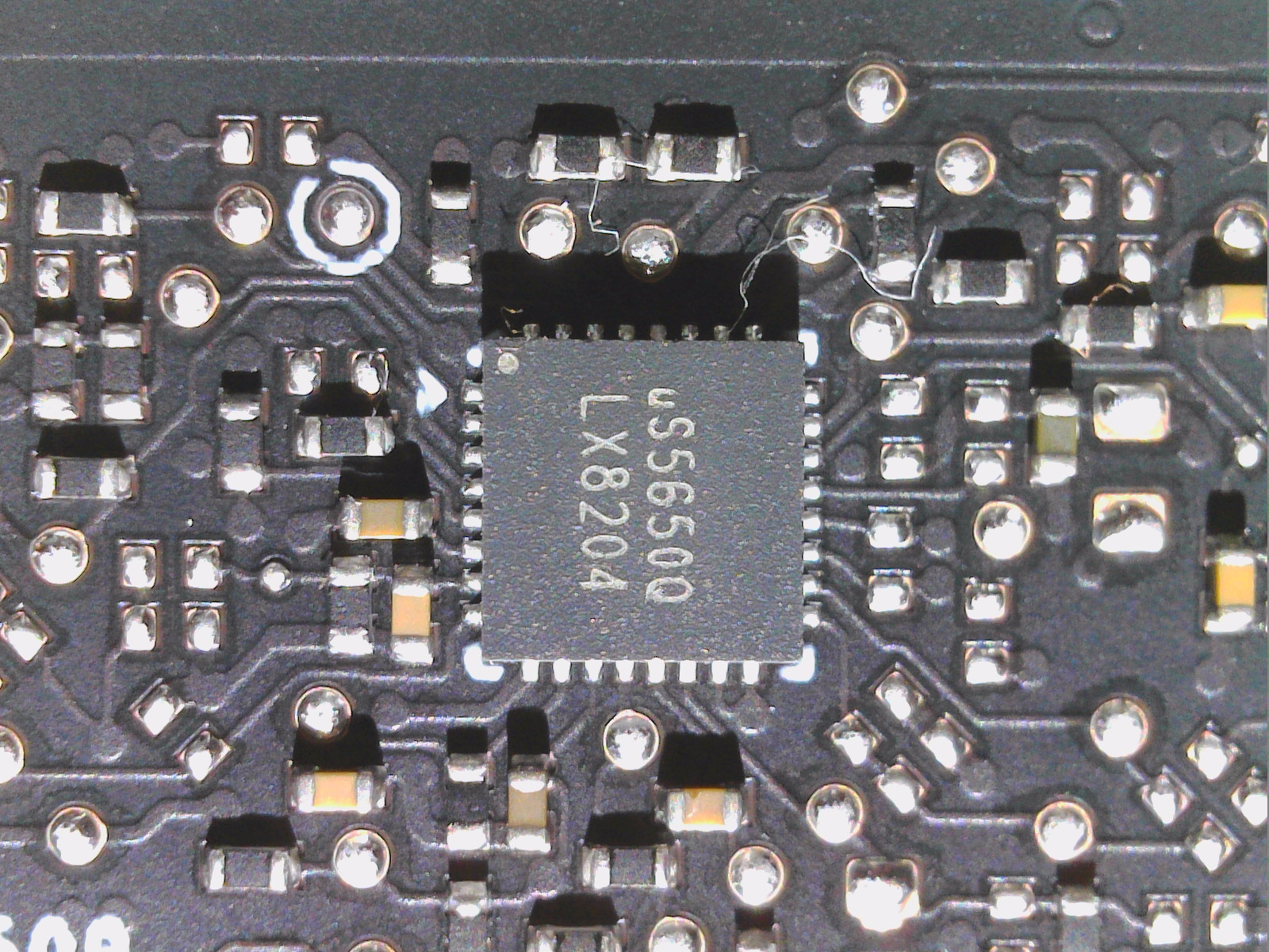
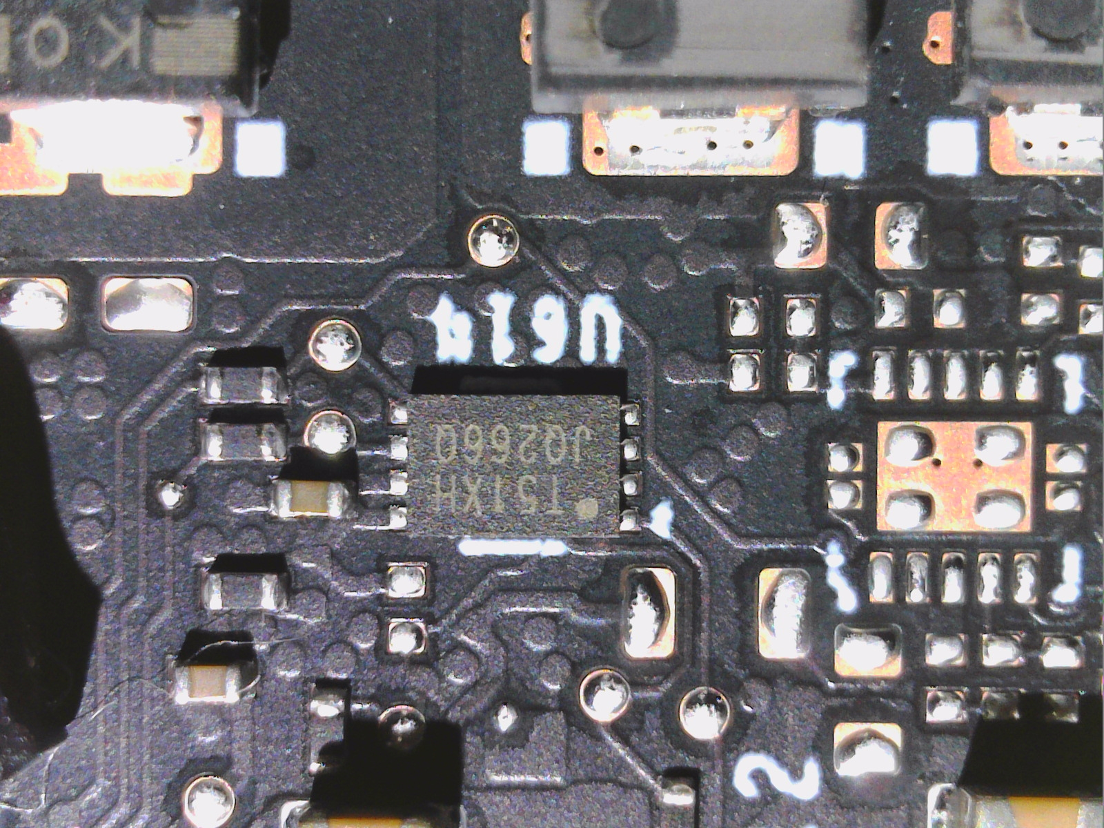
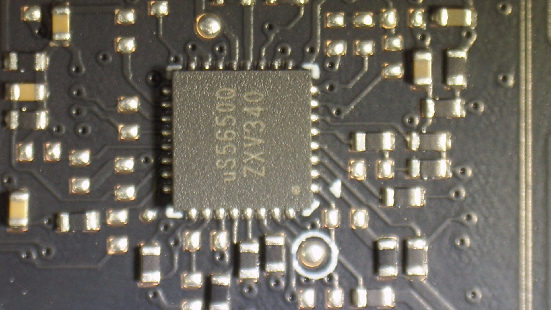
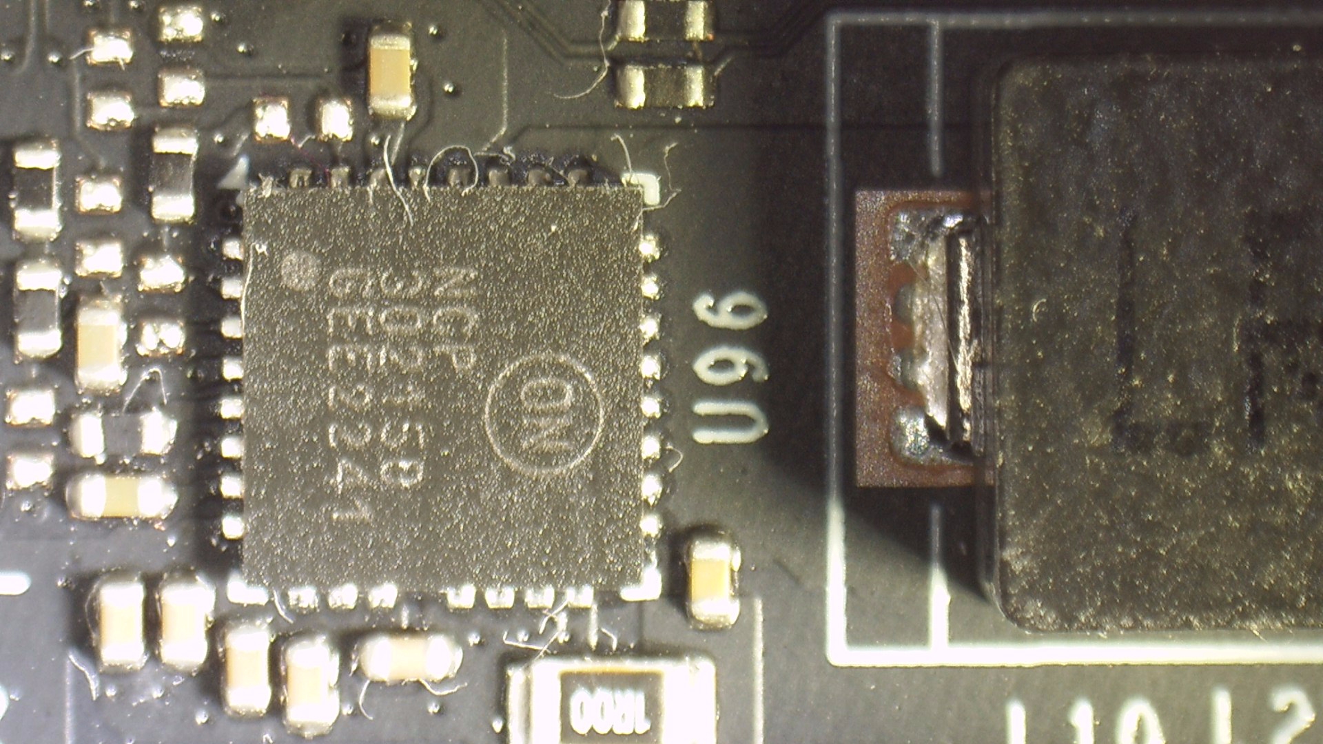
The joint PWM controller for NVVDD (GPU core) and FBVDDQ (memory) in the form of the MP2891 from Monolith is currently one of the top models among PWM controllers. It is a digital, multiphase dual-rail controller that primarily provides the power supply for the NVIDIA PWM VID core and is also compatible with the AVSBus interface. The MP2891 can (and should) also work with MPS’ Intelli-PhaseTMTM products to complete the multiphase voltage regulator (VR) solution with a minimum of external components. The MP2891 is even underpowered with the 10 phases on rail 1, as it could control up to 16 directly. The two phases for the memory are then controlled on rail 2 (up to eight would be possible there). The older RTX 4080 Non-Super still had three phases, but one has been deleted (gray). The chip is located on the back of the board. Right next to it on the left is a uPI uS5650Q for monitoring the four 12V rails (3x Aux and 1x PEG).
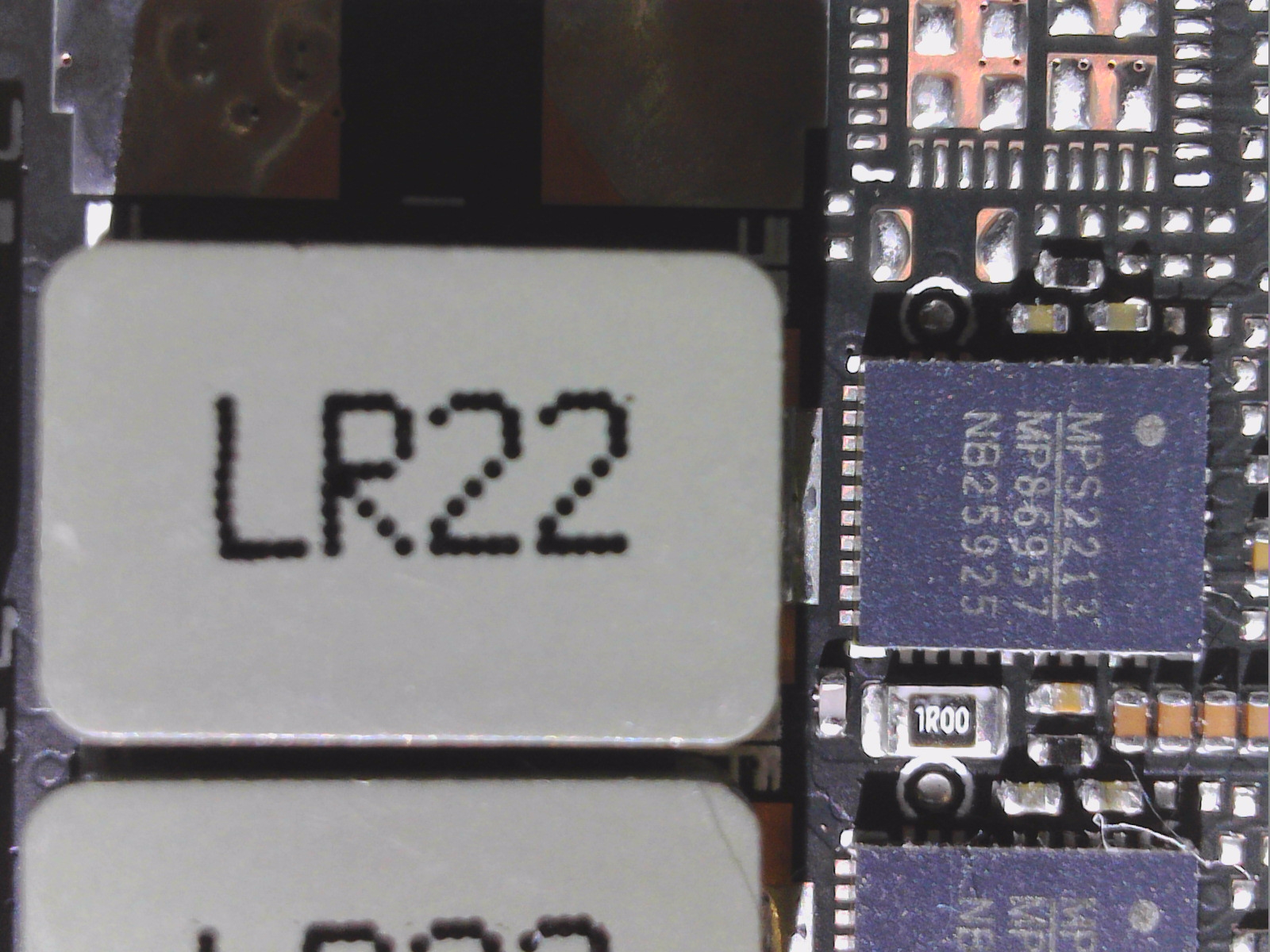
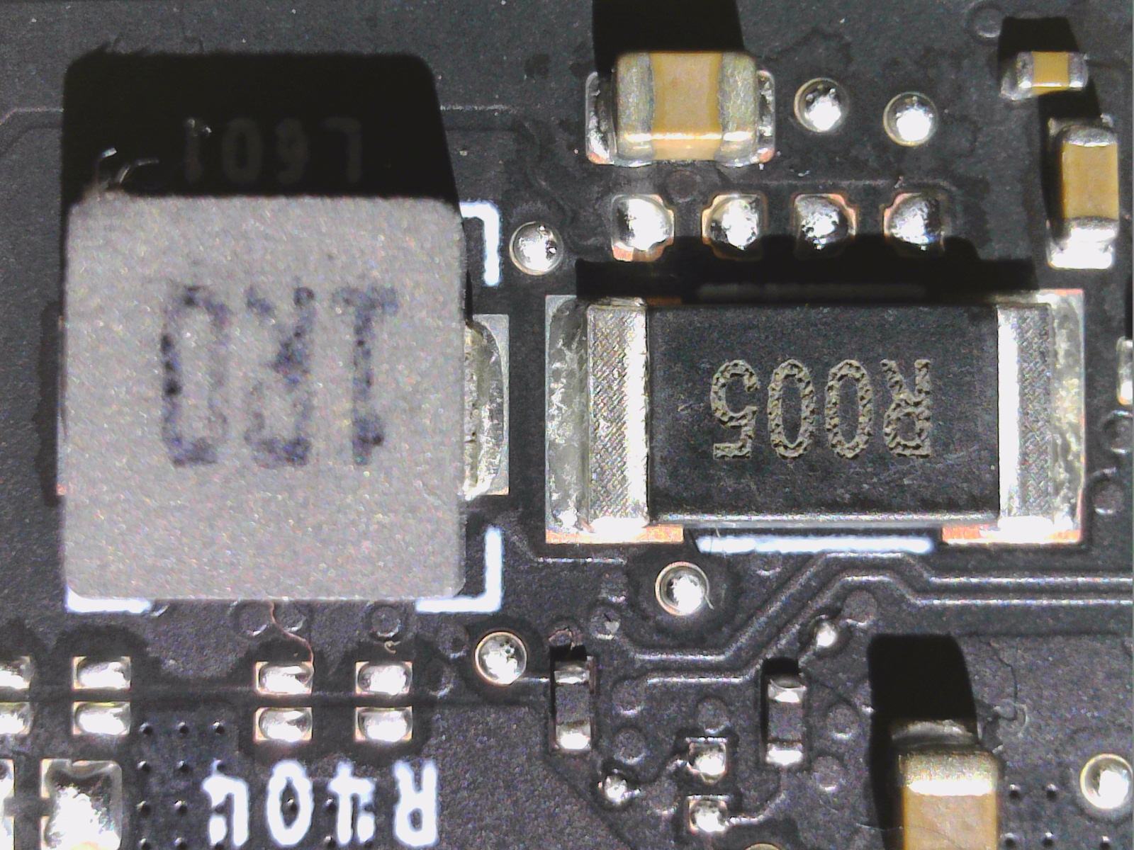
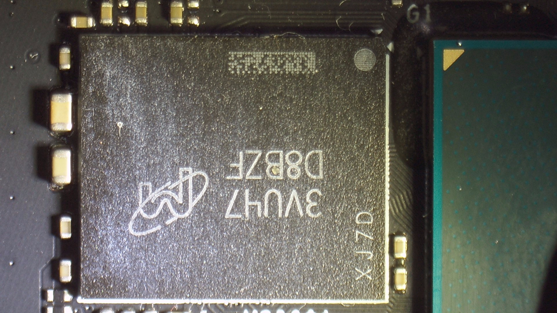
All power stages used, including those for the memory, are also products from Monolith. The MP86957 is a monolithic half-bridge that can drive up to 70A per phase. The integration of drivers and MOSFETs (DrMOS) results in high efficiency due to an optimized dead time and a reduction of parasitic inductance. This small, 5 mm x 6 mm LGA component can be operated at frequencies from 100 kHz to 3 MHz and is therefore ideally suited to the MP2891.
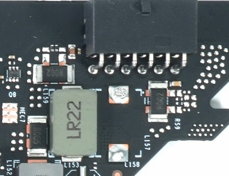
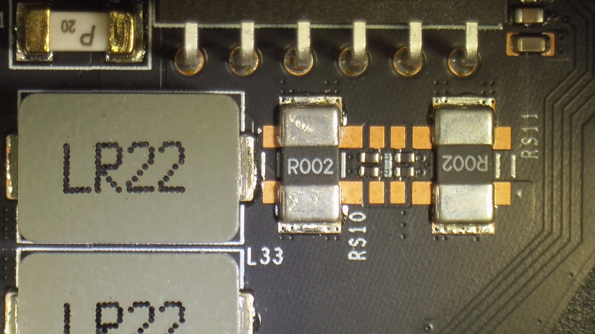
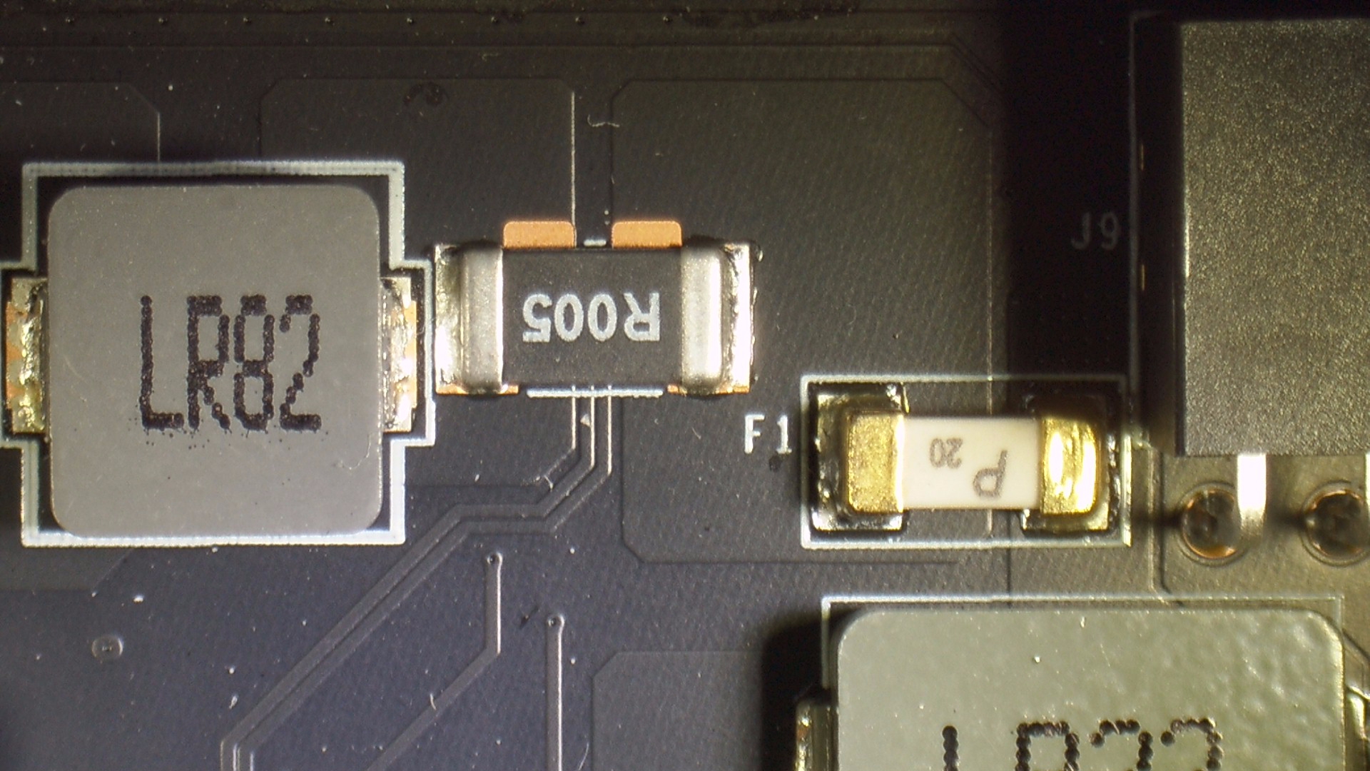
The two 12V rails on the 12 4 12VHPWR connector are combined into one rail after the two shunts (one per rail), another is connected to the PEG, but is not used for NVVDD. The single BIOS is in the usual place and the generation of the remaining low voltages is the same as before. So there are no other special features. The two ribbon cables for the fans are self-explanatory.

Teardown: PCB layout and components of the MSI RTX 4080 Super Expert 16GB
Let’s start with the PCB, which is completely new and remotely similar to NVIDIA’s shaped design. NVVDD is once again the most important voltage here, resulting in a voltage converter design with a total of 8 real phases and a total of 13 control circuits for NVVDD alone, some of which are connected and controlled in parallel (5x 2 phases 3x 1 phase)
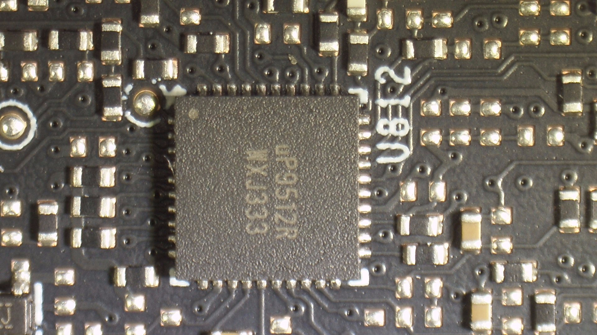
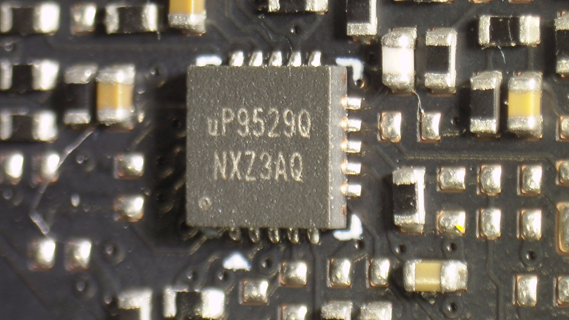
Once again, separate PWM controllers are used for NVVDD (GPU core) and FBVDDQ (memory), as the top models among the PWM controllers are unfortunately far too expensive. Therefore, the good and well-known uP9512R from UPI, which can only generate 8 phases, has to do the job again, which also results in the somewhat unusual circuit diagram. A second PWM controller in the form of the small uP9529 is then used to control the three phases for the memory. Both controllers are located on the back of the board. Directly between them is a uPI uS5650Q for monitoring the 12V rails (1x Aux and 1x PEG). These components are located on the back of the board
All DrMOS used, including those for the memory, are rather inexpensive products from OnSemi. The NPC302150 with 50A peak current used in all control circuits for NVVDD and FBVDDQ (memory) integrates a MOSFET driver, a high-side MOSFET and low-side MOSFET in a single package. This chip is specifically designed for high current applications such as DC-DC buck power conversion applications. This integrated solution reduces the footprint on the PCB compared to a solution with discrete components. The coils used for NVVDD and the memory have an inductance of 220 nH, the capacitors are solids in SMD design, which is slightly more expensive.
The 12V rails on the 12 4 12VHPWR connector are combined into two rail rails directly after the socket, another one is connected to the PEG and is only used very little for NVVDD. MSI uses various fuses in addition to the shunts, at least. The BIOS is on the rear and the generation of the remaining extra-low voltages is actually the same as before. So there are no more special features.

- 1 - Introduction, technical data and technology
- 2 - Unboxing and technical details of both cards
- 3 - Test system and measuring equipment
- 4 - Teardown: PCB and components
- 5 - Teardown: Cooler and fans
- 6 - Material analysis: NVIDIA RTX 4080 Super FE 16GB
- 7 - Material analysis: MSI RTX 4080 Super Expert 16GB
- 8 - Gaming-Performance WQHD (2560 x 1440)
- 9 - Gaming Performance Ultra-HD (3840 x 2160)
- 10 - Gaming Performance DLSS vs. FSR
- 11 - Gaming performance with Frame Generation
- 12 - Latencies and lags
- 13 - Workstation graphics and rendering
- 14 - Details: Power consumption and load balancing
- 15 - Load peaks, capping and power supply recommendation
- 16 - Temperatures, clock rates and infrared analysis
- 17 - Fan curves, noise level and audio samples
- 18 - Summary and conclusion


38 Antworten
Kommentar
Lade neue Kommentare
Veteran
Urgestein
Mitglied
Mitglied
Urgestein
Veteran
Veteran
Urgestein
Urgestein
Urgestein
Urgestein
Moderator
Veteran
Urgestein
Mitglied
Urgestein
Urgestein
Alle Kommentare lesen unter igor´sLAB Community →