


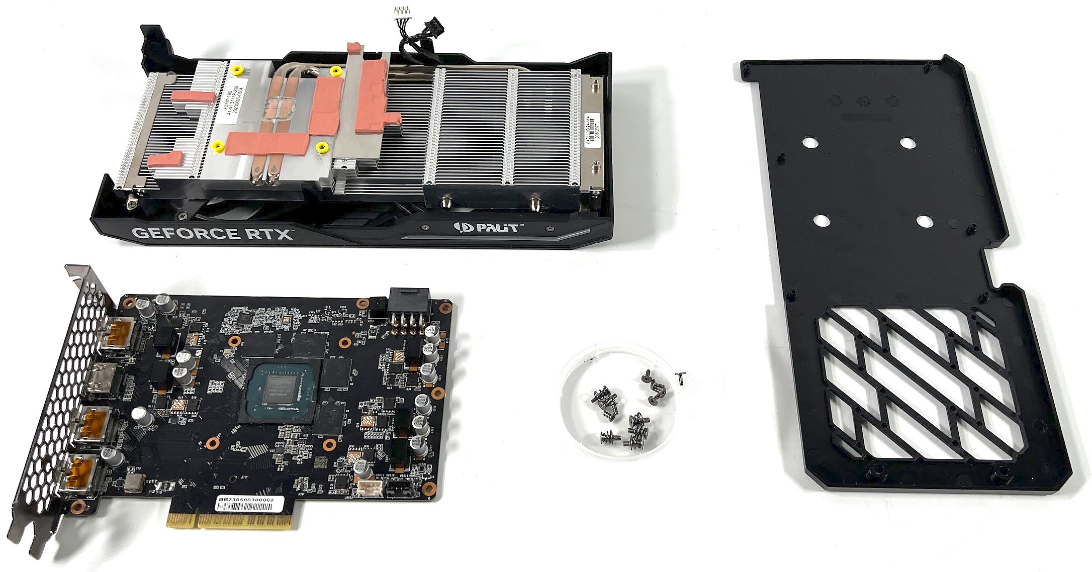
Teardown
The board is quickly disassembled, because where there is not much on it, there is not much to disassemble.
PCB layout and components
Let’s start with the PCB first. And this is where I got the first real shock. Yes, we are almost at the entry level, but what you get to see is pure cost down. NVVDD is the most important voltage and so it results in a voltage converter design with a total of four phases and the resulting control loops for NVVDD alone. Thus, you save another phase compared to the RTX 4060 Ti FE, but this is somehow still acceptable in view of the significantly lower TDP. Considering possible hotspots and a higher efficiency, more phases would certainly have made more sense. But it should also be about the price and so a compromise has to be made again.
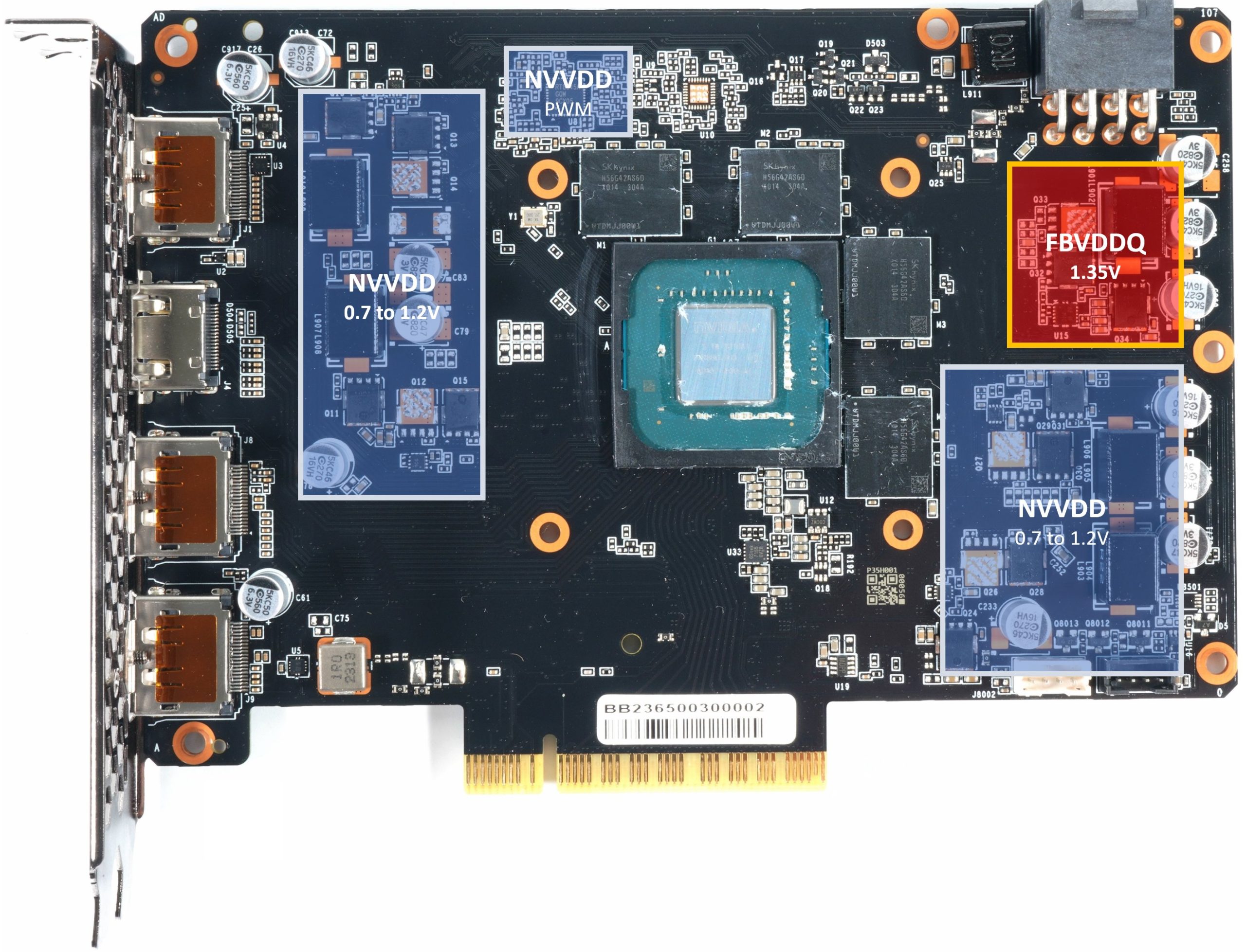
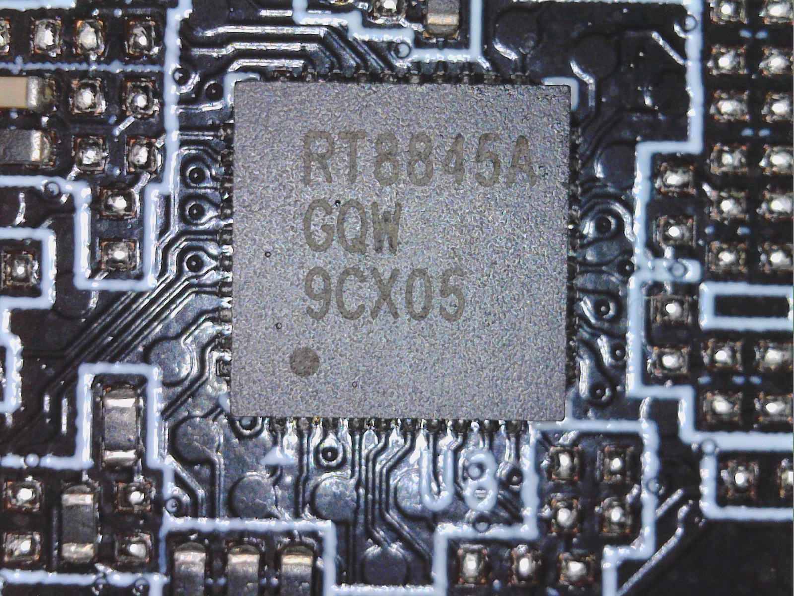
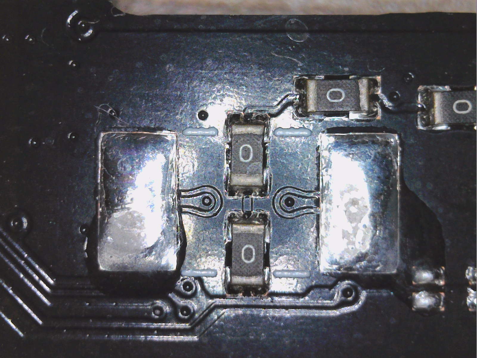
This all looks a bit too meager at first glance, but it’s enough. A very cheap PWM controller is used for NVVDD (GPU core), FBVDDQ (memory) is solved via a trivial buck converter. For NVVDD, Palit uses the cheap RT8845A from Realtek, which doesn’t get jinxed with the maximum of four phases, but gives away efficiency especially in the low load range. There are no DrMOS, the voltage converters are all discrete with N-channel MOSFETS and separate low and high sides.
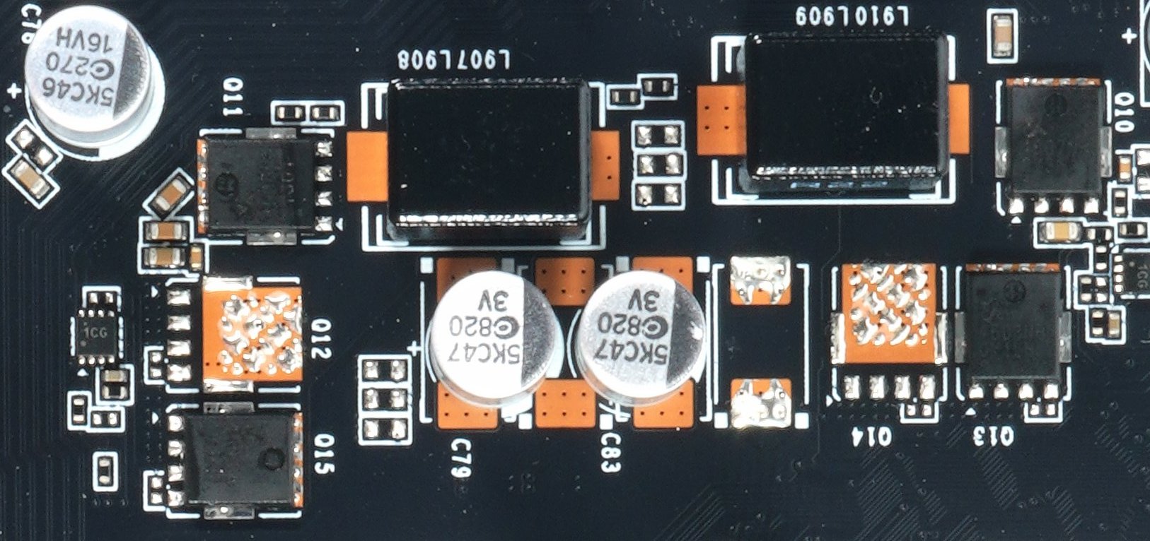
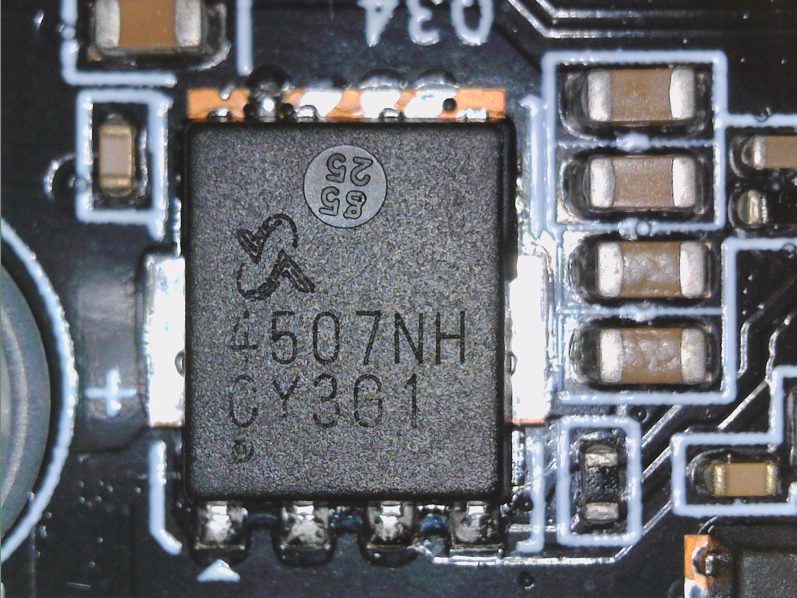
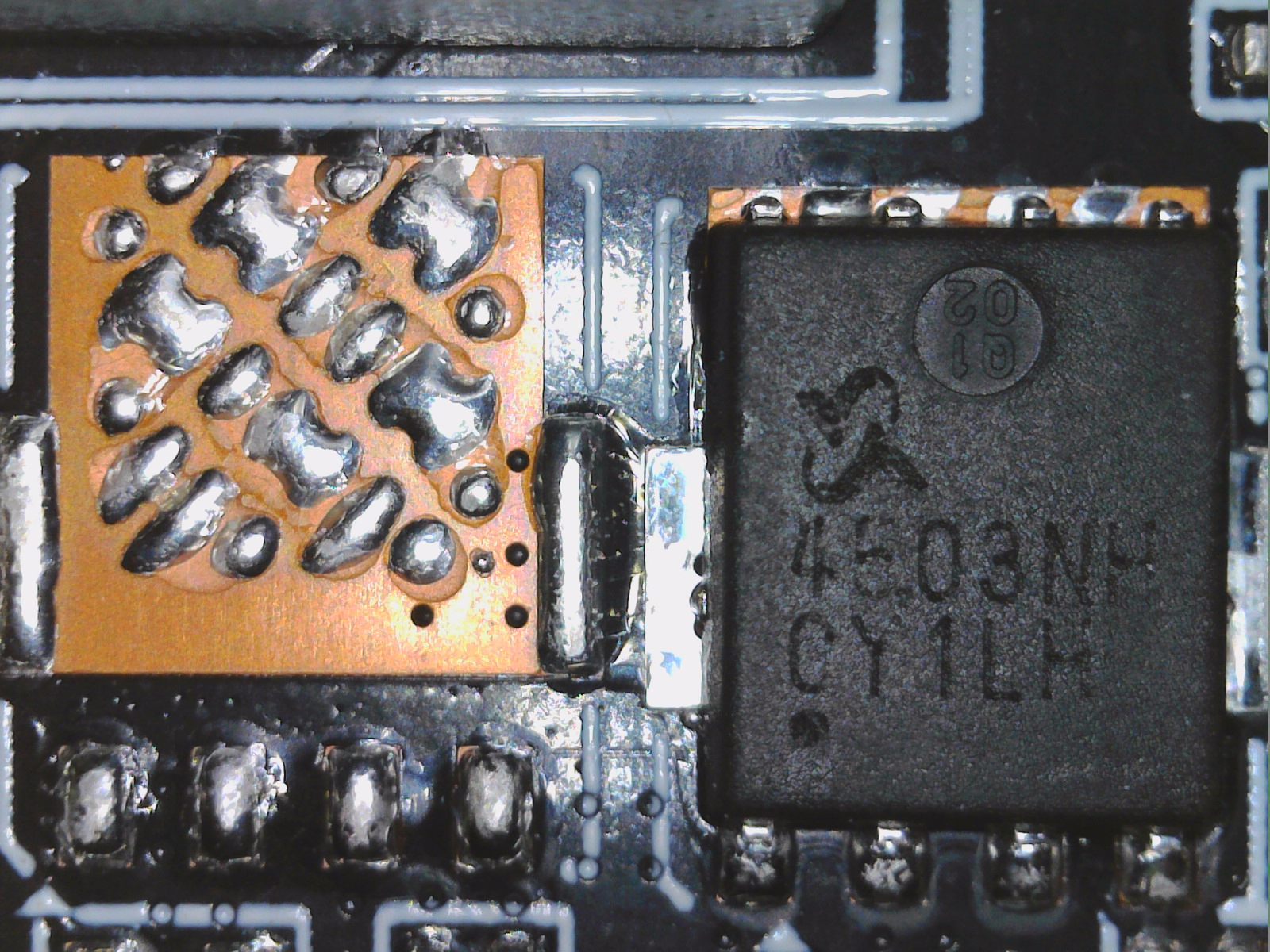
All MOSFETs used for NVVDD are low-cost products from Sinopower. The SM4503NHKP used in all control circuits for the low side is an N-channel enhancement mode MOSFET for a maximum of 80 amps. The RDS(ON) is typically 2.5 mΩ and can rise to 3.75 mΩ when fully heated. If an already provided parallel circuit had been used here, the losses could have been almost halved. The SM4507NHKP used in all control circuits for the high side is also an N-channel enhancement mode MOSFET, but rather not decisive for the power to be produced. It is driven by a separate gate driver.
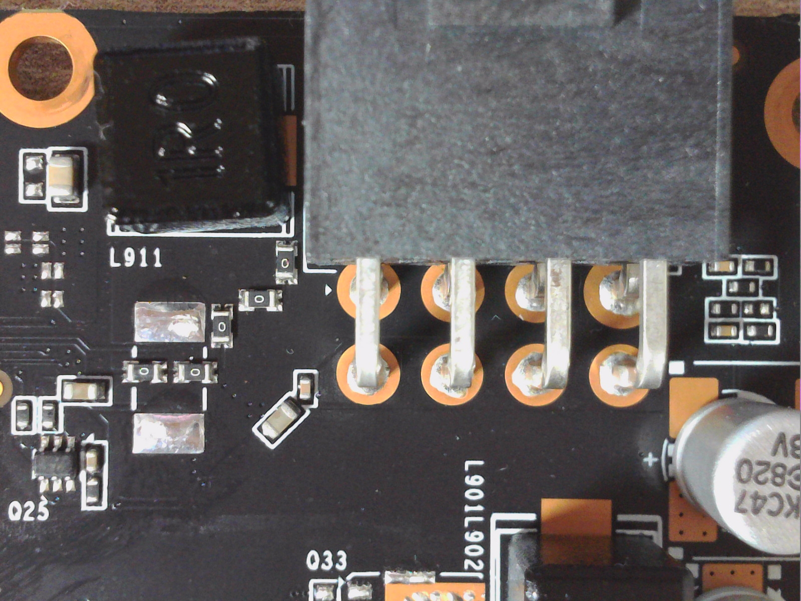
The one phase for FBVDDQ (memory) is also realized discretely and consists of the same MOSFETs as the four NVVDD phases. The 12V rails on the 6 2 connector are combined into a single rail just after the socket, another one is connected to the PEG, and is only slightly used for NVVDD.
Where is the control of the flowing currents? Kaputt gespart!
NVIDIA is actually known for permanently monitoring every 12V rail with shunts and the voltage drop that occurs there. Thus, a suitable monitoring chip can be used to determine the flowing currents and the firmware can then throttle the power supply so that the maximum power target stored in the firmware is never exceeded. Interestingly, these shunts do not exist on any of the RTX 4060 boards and a suitable monitoring chip is also completely missing.

NVIDIA declares the normal RTX 4060 as 115 watt cards and even talks about typical 110 watts when gaming. However, this is exactly untrue. Yes, the values that can be read via NVAPI are dutifully at 115 watts and below, but unfortunately they are not even close to correct. While the interface remains at 115 to 116 watts in the software, I actually measure over 130 watts on the rails and 4 games! That’s 15 watts more than the maximum allowed and still 20 watts above the communicated value for the games! Thus, the card is by far not as efficient as the interface suggests and the PR slides would like it to be. That would be over 18 percent more for gaming! But we’ll get to the exact values later and we see that not only the idle power consumption is a bigger construction site.
You need a special procedure to be able to control the single control circuits at all. The keyword is DCR (Direct Current Resistance). In the end, every component has very specific characteristics in this respect. To make it short: DCR is the basis for calculating or measuring temperatures and especially currents. But how does the controller find out exactly which currents flow in which control loop? The monitoring can be different, because there are – who is surprised – different methods for it.
We have already analyzed that the voltage transformers have been implemented at the technical level of 10 years ago. Intelligent Smart Power Stages (SPS), which measure the drain currents of the MOSFETS for the MOSFET DCR in real time, are pure utopia here. One replaces the whole thing with the much cheaper Inductor DCR in a discrete circuit, i.e. a current measurement via the inductive resistance of the respective filter coils in the output area. However, the accuracy of this solution is significantly lower and is also strongly influenced by fluctuations in the component quality. AMD has relied on this Inductor DCR for years, but it is no more than a rough estimate and becomes increasingly inaccurate especially at higher temperatures.
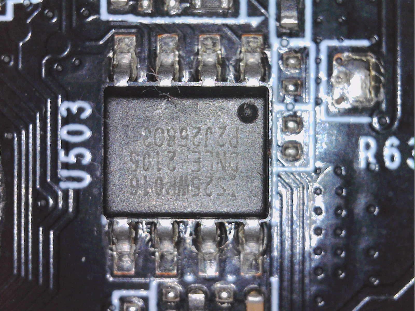
The BIOS is in the usual place and the generation of the remaining extra-low voltages is also as usual. So there are no more special features.

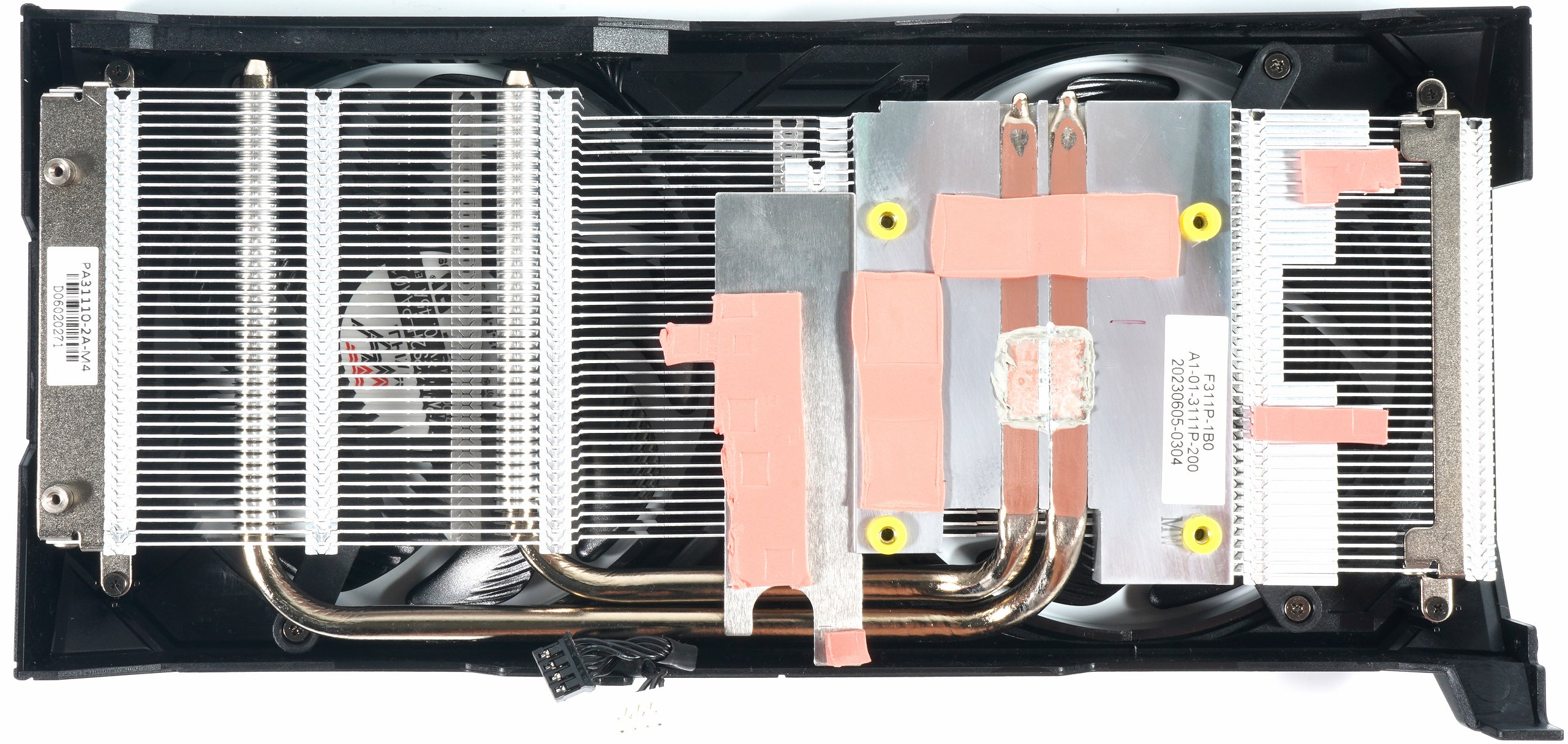
The cooler
The two 9.8 cm fans (opening 10 cm) have 9 rotor blades each and are controlled together. The usual second control curve is unfortunately omitted on the GeForce RTX 4060. Palit uses a simple fin heatsink in horizontal design and two 6 mm DHT heatpipes made of copper composite material pressed into the aluminum heatsink and ground. The pads are unfortunately not so high quality, but sufficient. If and when some silicone will leak there if necessary remains to be seen.
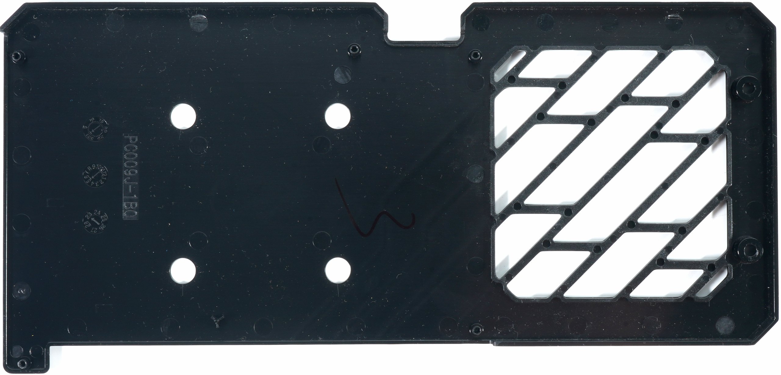
The backplate is made of ABS and only serves as stabilization. There is no need to report more here, because there is nothing.

- 1 - Introduction, technical data and technology
- 2 - Test system in the igor'sLAB MIFCOM PC
- 3 - Teardown: PCB, components and cooler
- 4 - Gaming performance FHD (1920 x 1080)
- 5 - Gaming performance WQHD (2560 x 1440)
- 6 - Gaming performance DLSS vs. DLSS3 vs. FSR
- 7 - Latency and DLSS 3.0
- 8 - Power consumption and load balancing
- 9 - Transients, cutting and PSU recommendation
- 10 - Temperatures, clock speeds, fans and noise
- 11 - Summary and conclusion


44 Antworten
Kommentar
Lade neue Kommentare
Neuling
1
Neuling
Neuling
Urgestein
Moderator
Urgestein
1
Urgestein
Urgestein
Veteran
Mitglied
1
Mitglied
Urgestein
Urgestein
Urgestein
Mitglied
1
Alle Kommentare lesen unter igor´sLAB Community →