


Measurement of the internal temperature (circuit board)
Since the PCB is directly thermally connected to the case via a good pad, the delta between the PCB (or the copper bridges in the 12V string) and the outside can also be extrapolated, since the thermal conductivity, thickness and area of the pad are known. For this measurement, I aligned the calibrated PI640 perpendicular to the top of the adapter, where the black stripe of the special measurement tape with a known emissivity lies just above the thermal pad. I will measure the front of the adapter including the back of the graphics board later. All measurements are made after a warm-up period of at least 30 minutes, the card is cooled with a chiller and constant 20 °C water temperature. Thus, the conditions are also always the same.

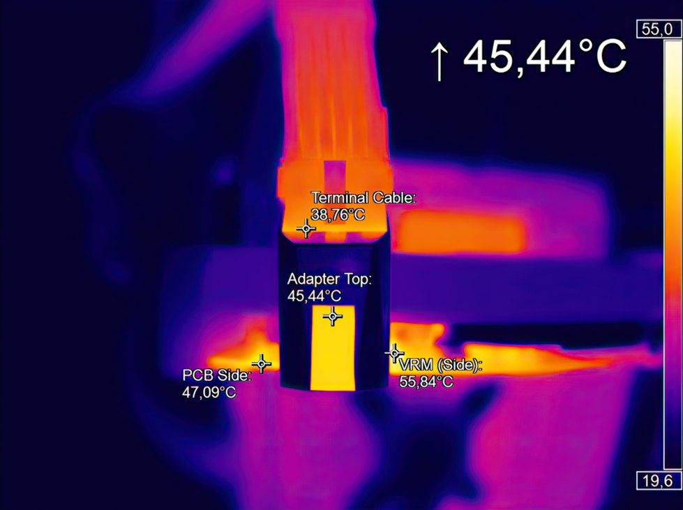
The adapter board, including the plug-in contacts, doesn’t even get hot at the normally maximum 450 watt load. We have a delta of about 2 degrees between the surface and the PCB or the contacts, so we can assume about 47 °C inside. This value is also shown by the control measurement of the board at the top edge. But what happens when the power limit of 600 watts is fully utilized?
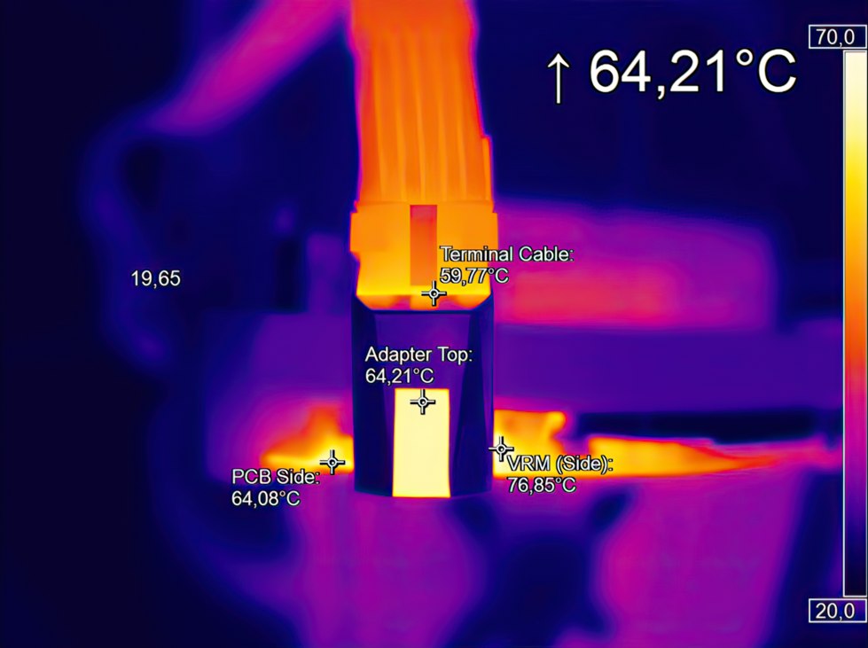
I now measure 64 °C at the adapter, the same value as at the checkpoint. We’ll see why this is important in a moment. Inside, we are at around 66 to 67 °C, which I logged using an inserted temperature probe. Thus, we can also assume the same delta between outside and inside here.
I recorded the entire process over 30 minutes and then uploaded it as a 30 second time-lapse video. You can see the slow heating up to the end point very clearly:

Measurement of board temperatures in the transition to the terminal
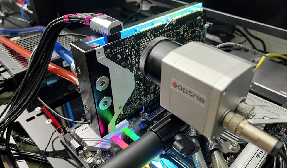
But how much do the contacts heat up additionally now? I now measure the back of the graphics card again and simply rotate the setup by 90 degrees. The PCB was again coated with a calibrated medium at the relevant points: transparent, silky matte measuring lacquer, as used for the “tropicalization” of PCBs. The familiar tape is stuck to the adapter again.
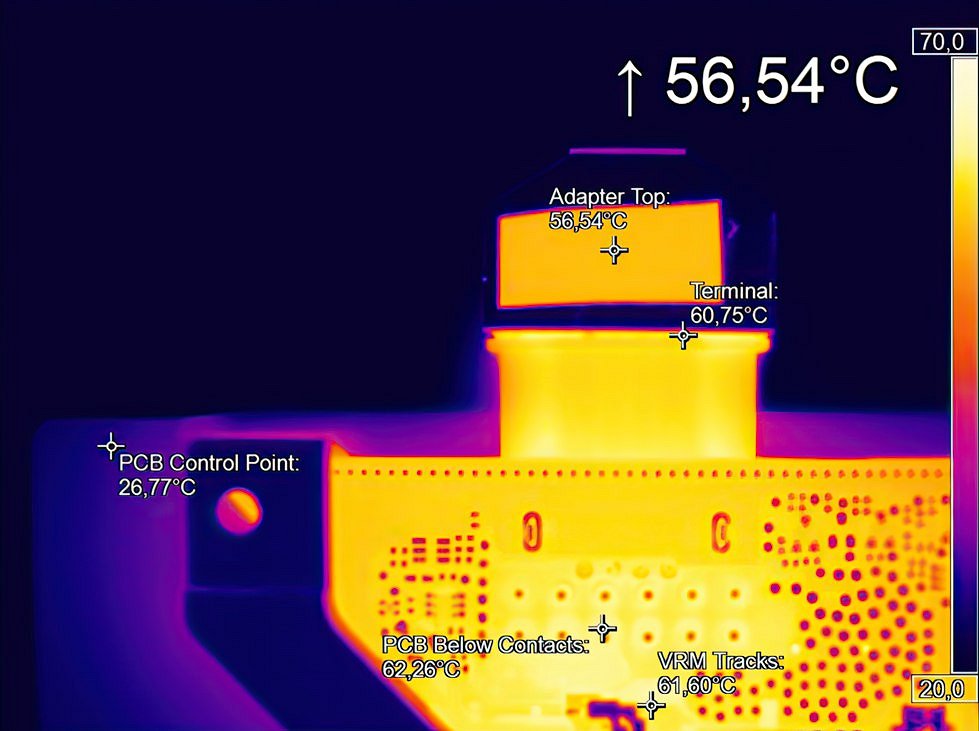
Let’s have a look at the soldering eyes of the 12V pins (PCB Below Contacts). there are about 2 degrees difference to the surface of the measured adapter. Thus, the assumption of 66 °C for the contacts and the circuit board is absolutely plausible. So we can assume that the flowing current at the maximum load warmed up the contacts, which were already warmed up by the graphics card, by another 4 degrees. Thus, the real waste heat caused by the contact resistance is only responsible for an increase of another 4 degrees, which is almost negligible!
To prove that the main part of the adapter’s heating is caused by the graphics card, I have attached two video clips of the radiometric measurements. First, we see real-time heating for over 30 seconds as it “travels” from the voltage transformers, through the tracks in the PCB, to the solder eyes:
The second video is a special time-lapse video that summarizes the 30 minutes (without the first 30 seconds) in 30 seconds again:
Interim summary
It’s all in the deep green range and the normal probes (inserted resistors) don’t say anything different than our non-contact measurement. And there are highly interesting, further findings after I also connected a lot of other things like native 12VHPWR cables or even NVIDIA’s adapter and then measured under load long enough. But that will be a new article, because it would simply go too far here. And yes, it could make a difference and also change things in production. So just stop by again this week.


568 Antworten
Kommentar
Lade neue Kommentare
Urgestein
1
Urgestein
Mitglied
Veteran
Urgestein
Mitglied
Urgestein
1
Urgestein
Veteran
Urgestein
Veteran
Urgestein
Urgestein
1
Veteran
Mitglied
Mitglied
Alle Kommentare lesen unter igor´sLAB Community →