


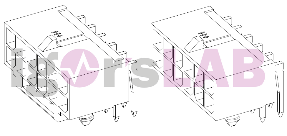
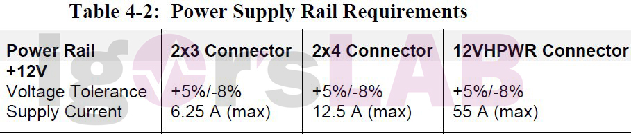
The 12VHPWR connector with and without sense pins
First, let’s take a look at the new connectors for the external power supply (Auxiliary Power), also known as the 12VHPWR connector. I already reported in detail about the 12+4 pin connector months ago, but there is also a “normal” 12-pin without the 4 sense pins, as used on the GeForce RTX 3090 Ti, which can also deliver up to 600 watts. Don’t be fooled by the fact that a 12-4 pin connector is usually already installed on the cards (because of the later power supply compatibility). The matching connector of the adapters to 3x 6+2 pin is only a 12 pin connector without sense pins and the 4 sense pins on the GeForce 3090 Ti are not connected. But both ports have one thing in common, because they currently also define the graphics cards with more than 300 and up to 600 watts of power consumption.
The MSI RTX 3090 Ti I tested already has a 12+4 12VHPWR socket soldered and partially also connected to the two center sense pins. The yellow marked pin S2 is for CARD_CBL_PRES# (cable connected) and the red marked pin S3 is for Sense 0. In this case 600 watts are specified only if the pin is connected to ground. But is it actually?
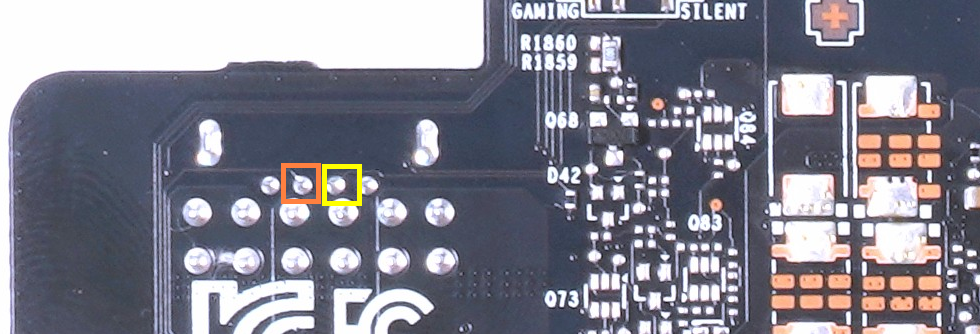
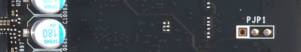
Interestingly, the trace does not end directly on ground (as suspected), but on a prepared, but not assembled power jumper (PJP 1) on top of the PCB. If you follow the PCI SIG specs for PCIe 5.0, then only 450 watts are actually enabled here. However, the card swallows up to 500 watts, so it would permanently exceed the standard by 50 watts. Now, you could of course ask yourself the counter question, what will actually happen when you then connect this card to a specified power supply in two years that could only recognize the graphics card as a 450 watt model. Whereby pin 1 for CARD_PWR_STABLE is also not assigned, so that a smart communication with a power supply via the power budget would not be possible at all. So the current state is not really definitive, which in turn rather points to the development playground already mentioned so often.
Graphics cards with 300 to 600 watts: new tolerance ranges for load peaks and the ratio
The most important thing in the current standardization up to 600 watts is first of all the so-called Combined Power, which precisely specifies that in the sum of external PCIe power supply (Aux) and the PCIe motherboard slot (PEG), no more than 600 watts may be called up as an average continuous load. It does not matter which rail delivers how much power in detail and the usual adding of the partial values of all rails is obsolete.
Furthermore, these standards listed below and called for by NVIDIA and AMD together only apply to graphics cards in the 300 to 600 watt ranges; the ranges below that remain as usual. Intel’s current silence could of course also be due to the fact that they don’t see any reason to even think about these load ranges because the new Arc generation is below them. I will also discuss PCI power management and power budgeting in a later article, but that would go too far here for now, especially since there are no really suitable power supplies officially available yet. However, in order to understand the remainder of this paper, we need to clarify or correct three terms that will be used repeatedly in the remainder of this paper. Then it will also work with the voltage peaks.
- Sustained Power – Average power in a time frame of 1 second or more
- TDP – Thermal Design Power is the maximum continuous power output
- Power Excursion – A temporary condition in which the power exceeds the maximum continuous power
In general, TDP and Sustained Power can be equated, so I will generally use the term Sustained Power here in the following. I had already mentioned on the first page that different power levels are defined for different time intervals in the individual overload ranges. Since this applies to all graphics cards in the range between 300 and 600 watts regardless of their Sustained Power (also TBP at NVIDIA or TDP at AMD), you can’t work with absolute wattages, but have to define a ratio between the average load measured in the respective interval and the Sustained Power.

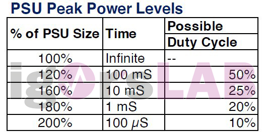
The following diagram now shows very clearly where the journey is heading for the individual intervals. From one second and more, the ratio of 1 applies, which is why the average power consumption may then no longer exceed the TDP. The other limit is 100 µs, where the one ratio of 3 allows even three times. With the interval used by many power supplies for the supervisor during monitoring of 20 ms the ratio is 1.25. And now at the latest, we also notice that the tested MSI RTX 3090 Ti SUPRIM had a ratio of 1.2, which is certainly anything but a coincidence. Thus, one calculates with an overload of maximum 375 watts at 300 watts to guarantee safe operation here. At 10 ms, you would then be back at 600 watts and the abnormal values that the older cards still reach. The question is what the power supply manufacturers will actually implement.
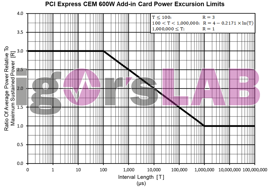
A ratio of 2.5 would even be allowed in not really that rare load peaks around 1 ms, which would result in 750 watts with the 300 watt TDP used as an example. We can already see: the load ranges that Intel communicated in a briefing as a guideline to the power supply manufacturers at the time are not that far off. This is for the people who accused me of nonsense and click-bait, because they simply didn’t know any better. Here again the little refresher:
Power consumption and load peaks as an extreme mix
If you don’t want to scroll through everything again, I’ll now show you the small excerpt of what Intel has given the manufacturers for 2022 and I’m still amazed by the numbers. For those who don’t know, CEM means PCI SIG Card Electromechanical, i.e. the plugged-in add-in cards. The CPU manufacturer estimates between 275 and 300 watts for the CPU, which is, however, plenty generous. However, I have also managed to squeeze far more than 300 watts into a Core i9-12900KF, which quickly puts the generous rating into perspective again.
The power consumption values of the graphics cards are also anything but utopian, because even without OC, AMD’s and NVIDIA’s new flagships are rumored to have around 500 to 600 watts of real board power. Woe betide if there is still overclocking leeway then. The estimation for the rest of the system is rather inconsistent, as the 100 watt approach is already a bit tight with motherboard power consumption of up to 50 watts even in the lower range, while the 300 watts is a bit exaggerated for the largest system. In spite of everything, however, this should somehow work out in total, because much of what I have already written about the ratio coincides. The table shown here is also not my invention, but originates from Intel’s briefing documents:
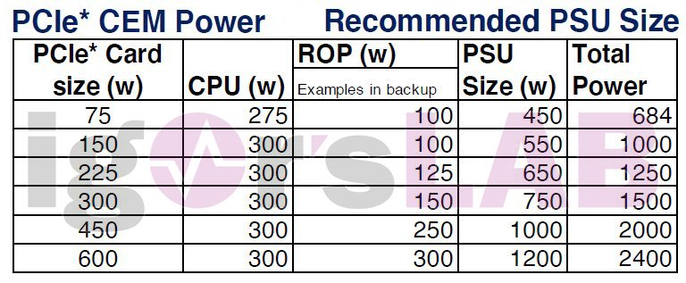
The estimated values for the PSU measurement (“PSU Size”) are thus clarified, but what is the Total Power all about? This is exactly what we need to talk about now, because it is exactly the part that worries me (and the power supply manufacturers) the most! Intel also has a defined idea for this and at the same time an announcement to the producers of the power suppliers. Let’s take a look at it now and get wide-eyed. Even if the length of the highest load peak intervals is limited to 100 μS each, the permissible total share of up to 10% of the total volume is downright abstruse. This means that the power supply must actually deliver 200% of the power over 10% of the operating time!
This actually turns the 1.2 kW power supply into a 2.4 kW power supply in disguise. This is because it is also defined in this way that normal operation can be at just 50% without a surcharge and the rest of the time can be blithely overloaded. Of course, this will all more or less amount to a pure single-rail solution as well, but from a purely electrotechnical point of view, this is outright madness. Which supervisor chip should still be able to realize a reliable protection circuit for OCP/OPP in a fixed defined interval here? Then what is still an allowable load and where does the emergency begin?
ATX v3.0 – Soften limits, close eyes and somehow through!
Even though some of the manufacturers might be able to produce such power supplies under the currently valid ATX specifications with the corresponding costs, the bar for the quality of the power supplies and the limits to be met is much too high for most of the cheap manufacturers. Or the products would then at least be so expensive again that acceptance would be completely zero. So you bend the whole thing a bit and even risk backwards compatibility. But let’s start again at the PCI SIG and see what they specify:
So far, so clear. And now the circle of the energetic show is closed, if we still include the transients. I know it was a lot of theory again, but I hope it came across well in spite of, or rather because of, deliberately breaking it down into more general terms. As already written several times, it refers to the upper performance class, which is of course also particularly thirsty. Whether you will really take part in this game as an end customer is up to you. In the end, it is also a matter of conscience.


15 Antworten
Kommentar
Lade neue Kommentare
Urgestein
Urgestein
Urgestein
Urgestein
Urgestein
Urgestein
Urgestein
Urgestein
Urgestein
Urgestein
Mitglied
Urgestein
Veteran
Urgestein
Veteran
Alle Kommentare lesen unter igor´sLAB Community →