


Teardown: PCB layout and components
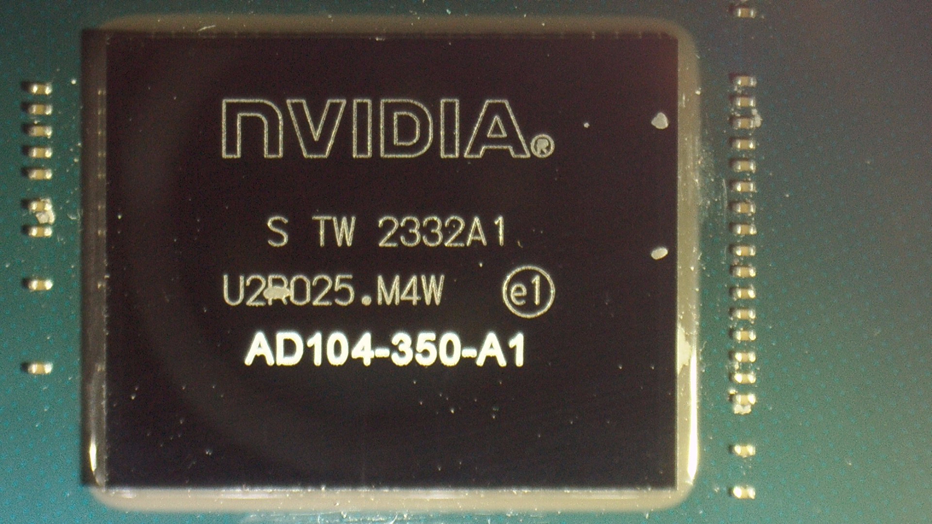
Let’s start with the PCB, which is 1:1 of the Non-Super’s PCB and even has the same revision number. NVVDD is still the most important voltage and this results in a voltage converter design with a total of 7 real phases and the resulting 7 voltage regulator loops for NVVDD alone. Compared to the RTX 4070 Ti, this is another significant saving, which is just about acceptable in view of the significantly lower TDP. I would have preferred eight possible phases and, in view of possible hotspots and higher efficiency, this would certainly have made more sense. But it’s also about the price and so once again a compromise had to be made. The PCIe slot as a power source would still have been enough, just for the record.
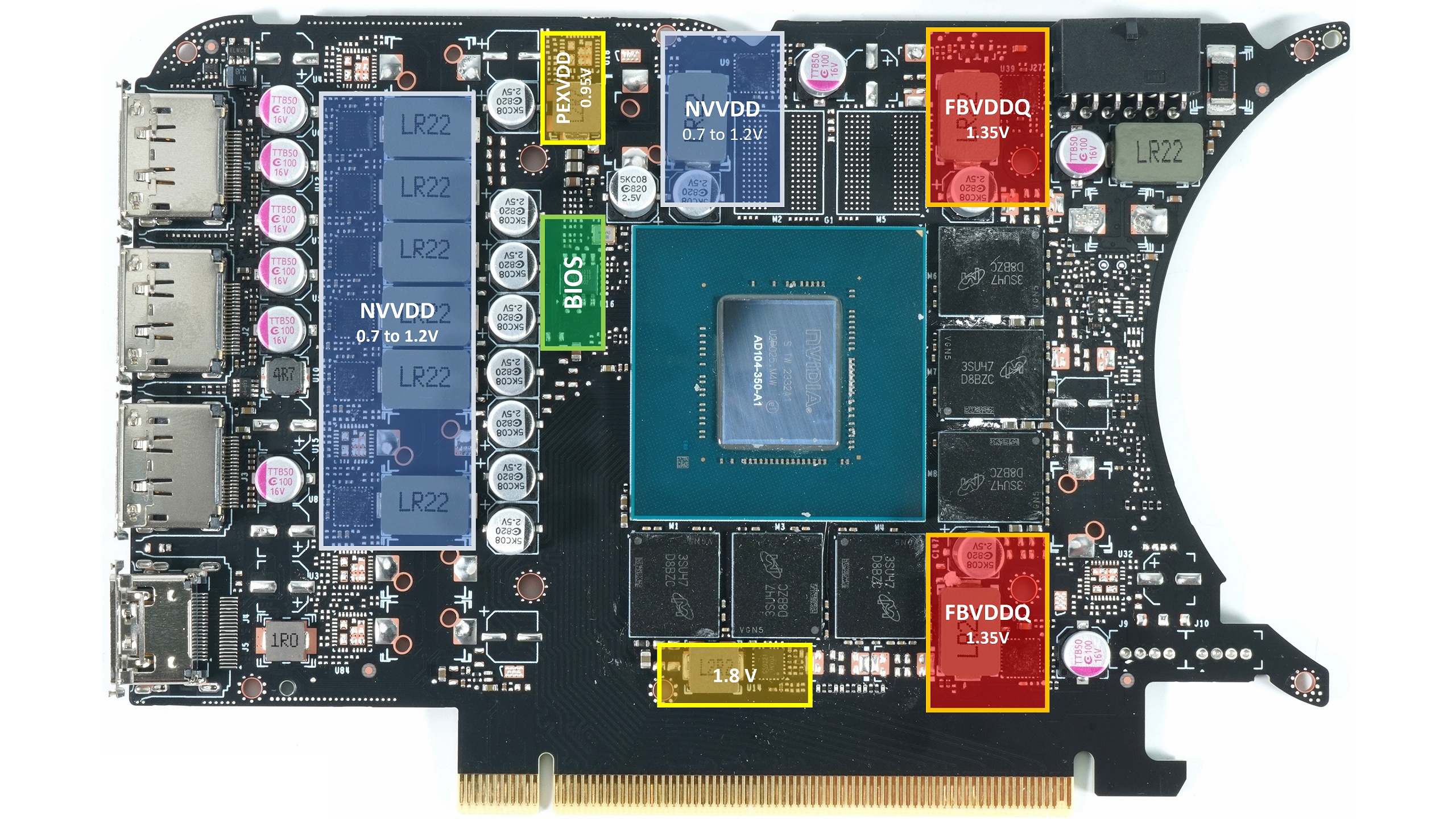
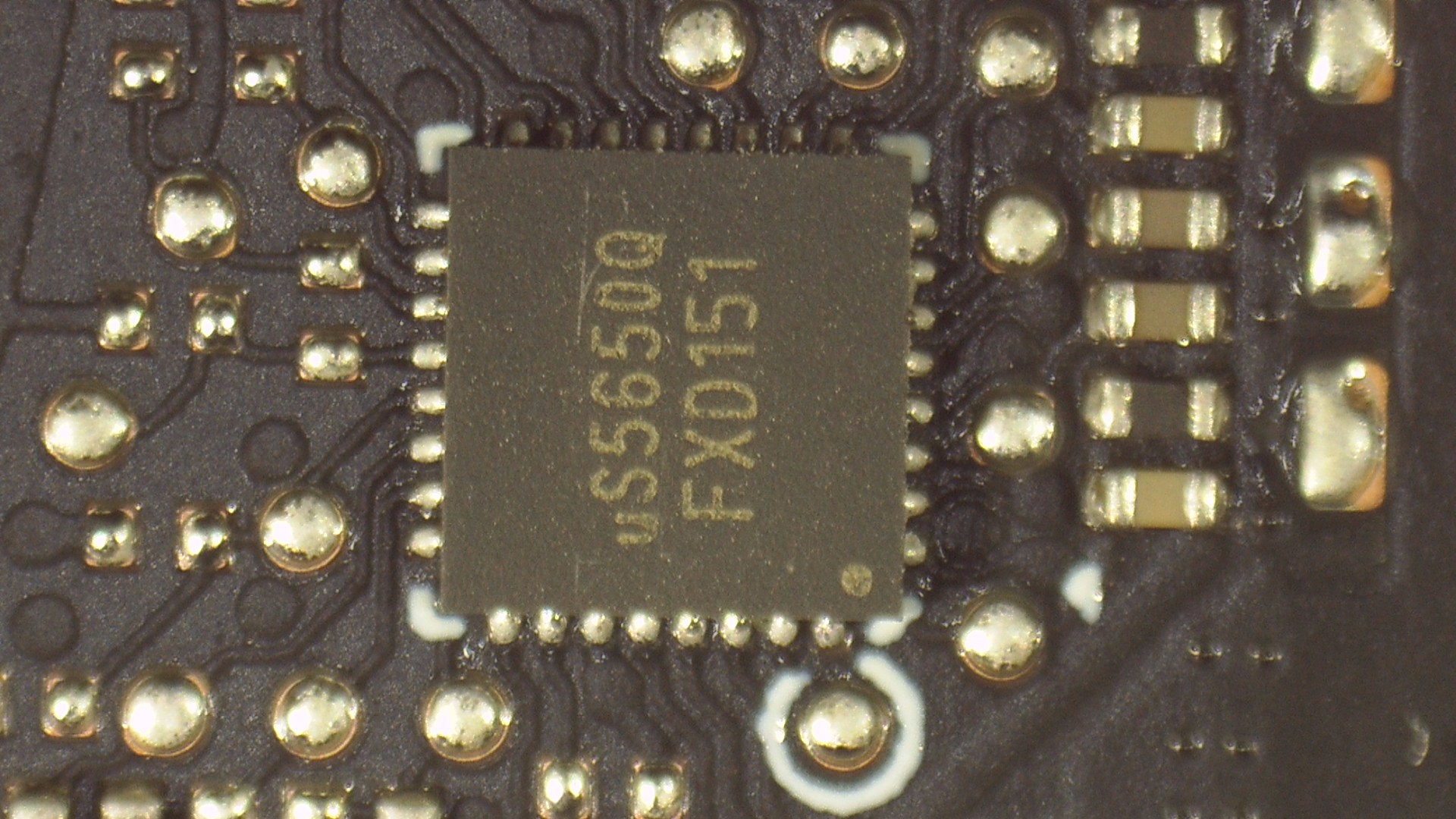
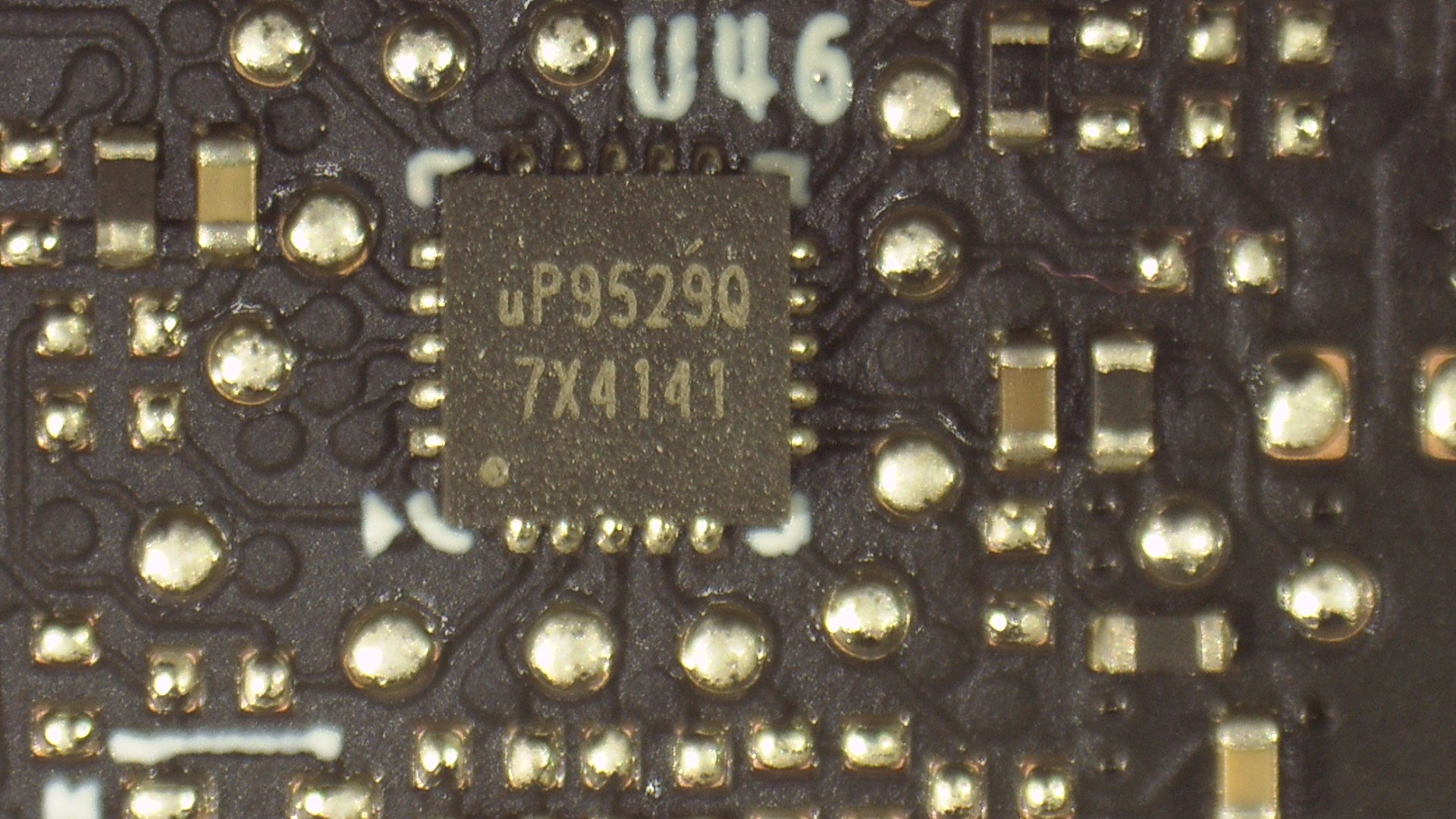
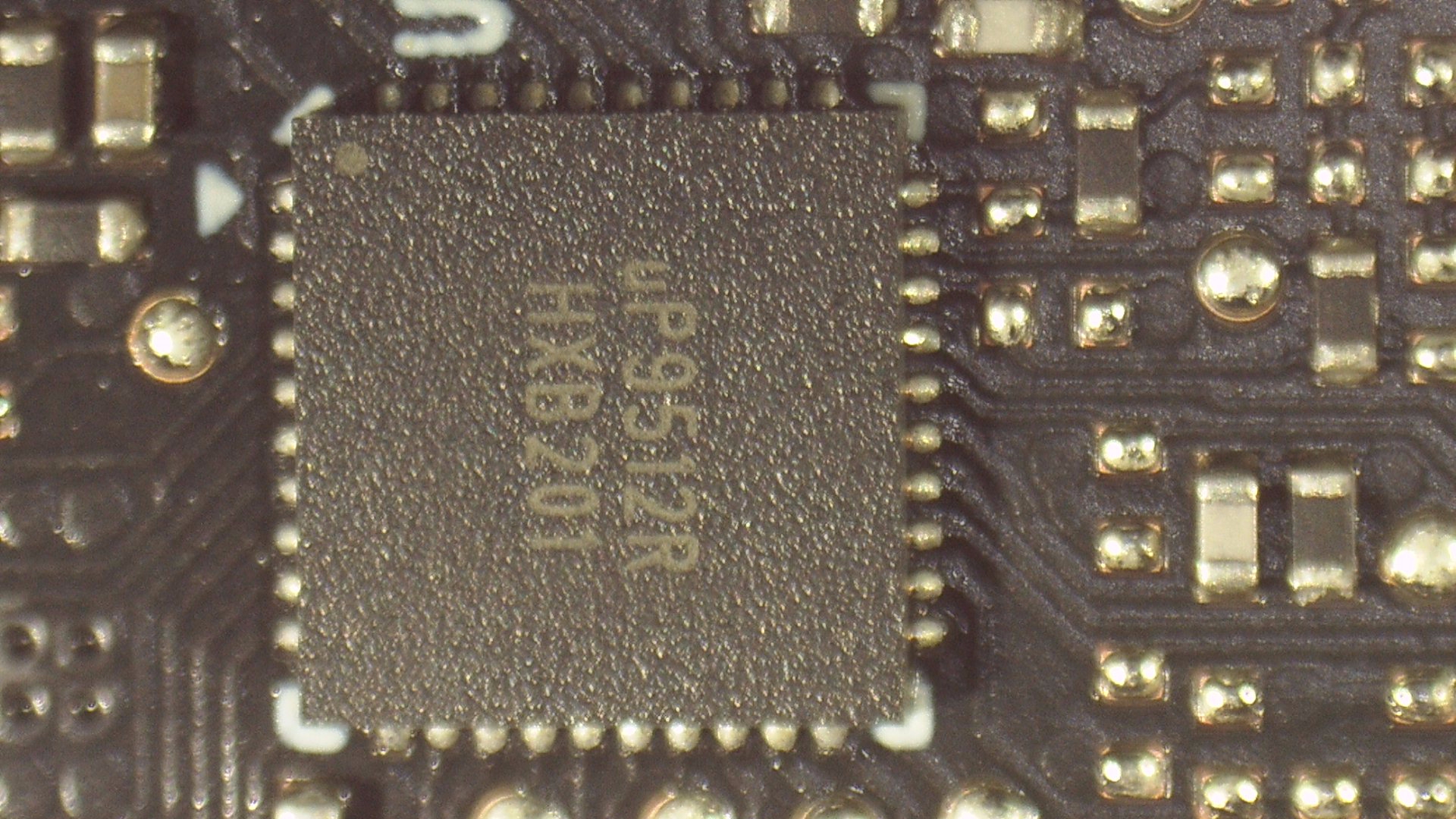
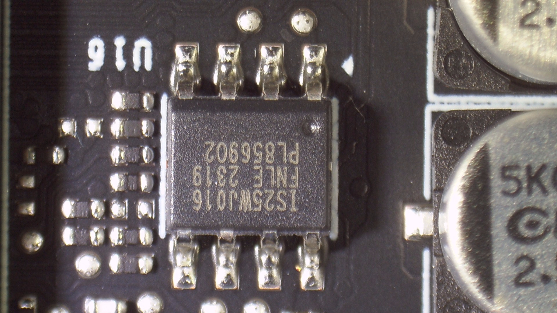
It all looks a bit meagre again, but we have to get through it now. Once again, separate PWM controllers are used for NVVDD (GPU core) and FBVDDQ (memory), as the top models among the PWM controllers are unfortunately far too expensive. Therefore, the good and well-known uP9512R from UPI Semi, which can only generate 8 phases and is significantly cheaper, has to do the job again. A second PWM controller in the form of the small uP9529 is then used to control the two phases for the memory. Both controllers are located on the back of the board. Directly between them is a uPI uS5650Q for monitoring the 12V rails (1x Aux and 1x PEG). So there is no difference at all between the Super and Non-Super.
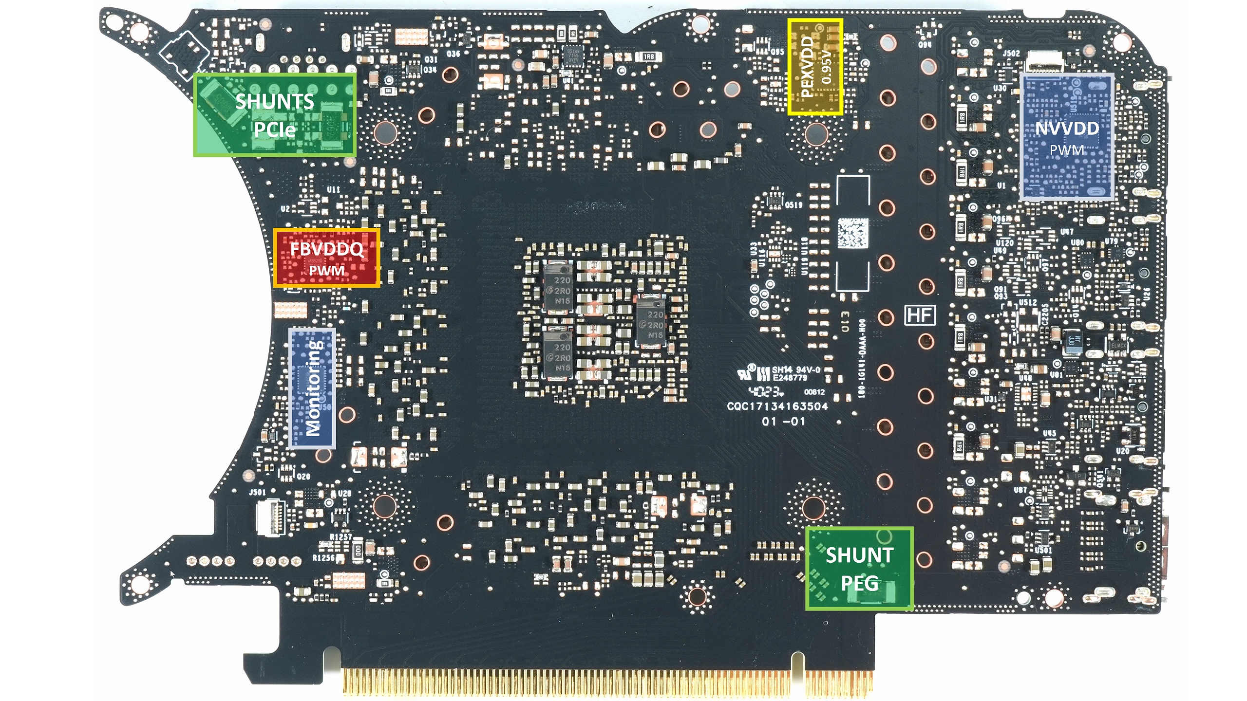
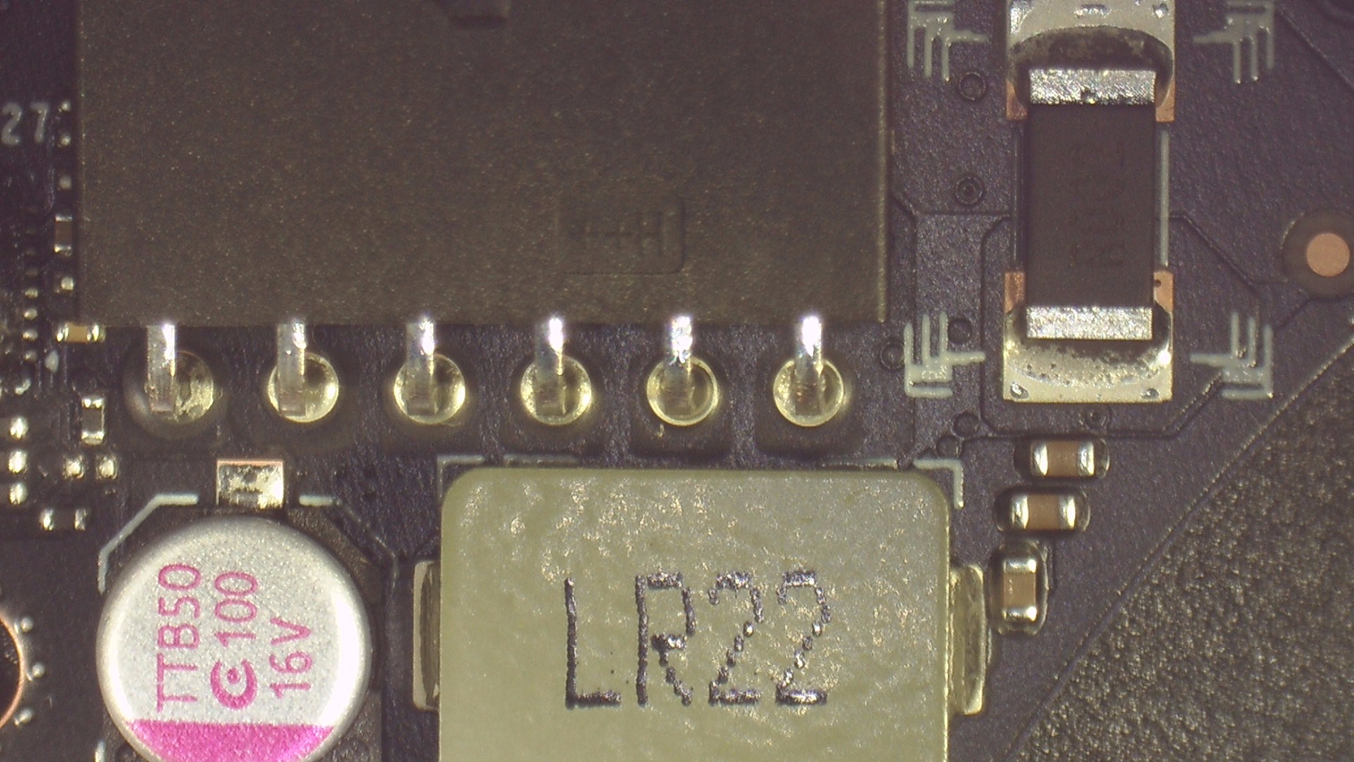
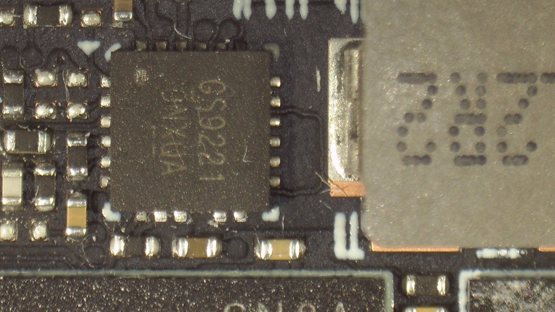
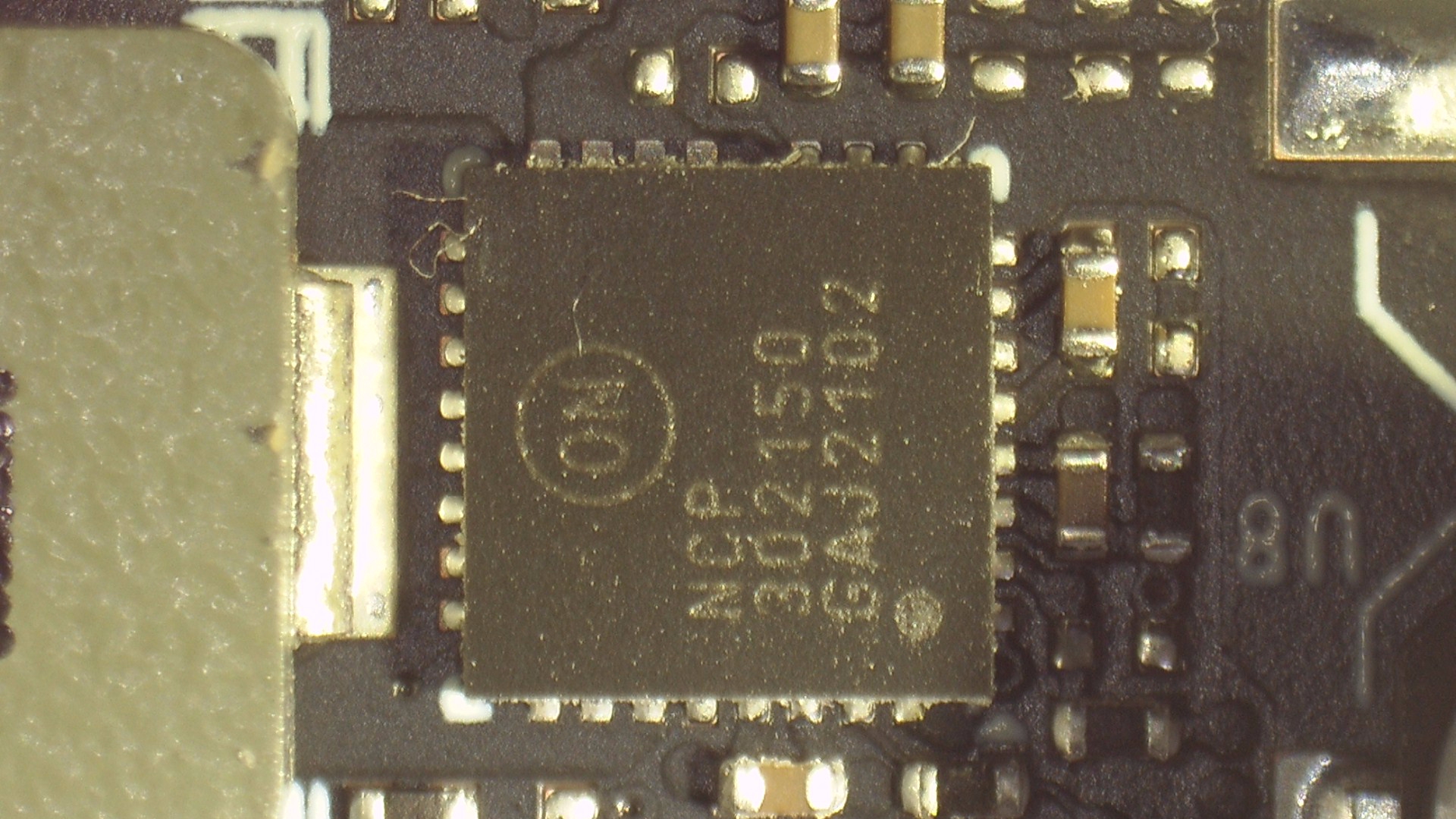
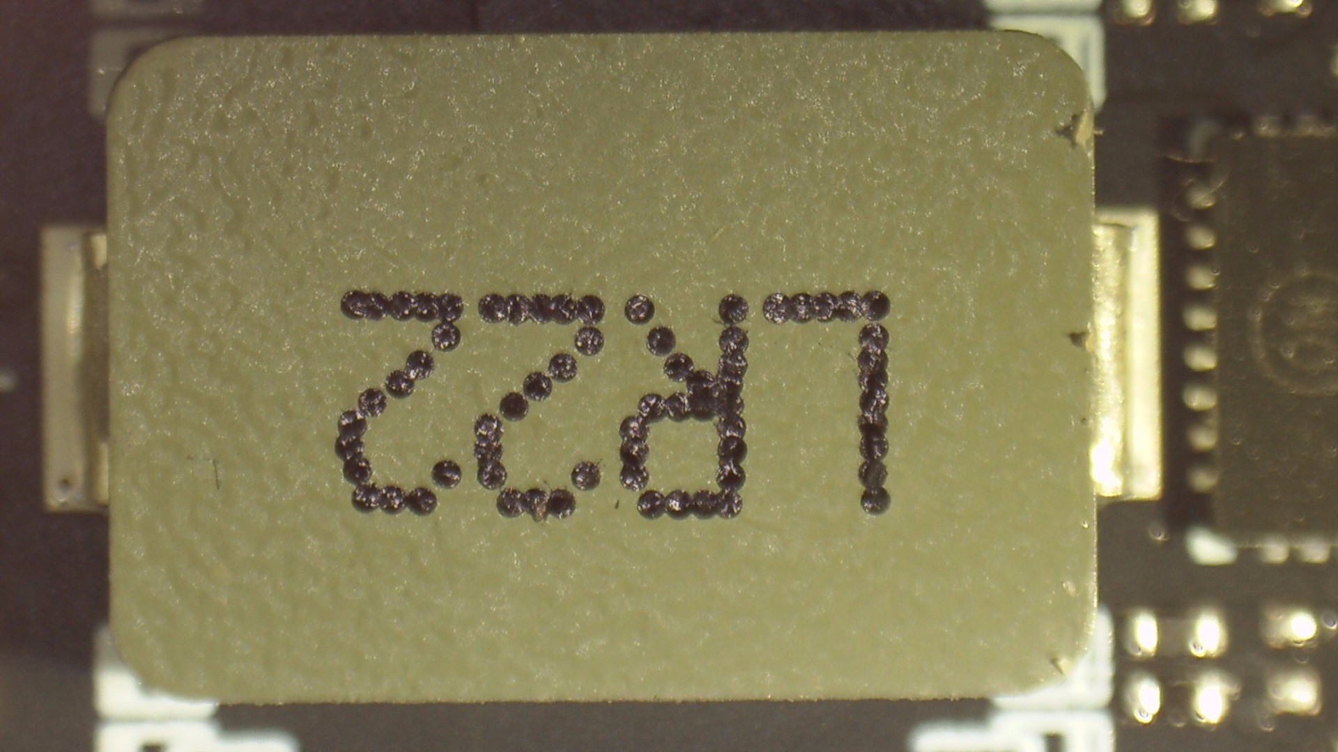
All DrMOS used, including those for the memory, are rather inexpensive products from OnSemi. The NPC302150 with 50A peak current used in all control circuits for NVVDD and FBVDDQ (memory) integrates a MOSFET driver, a high-side MOSFET and low-side MOSFET in a single package. This chip is specifically designed for high current applications such as DC-DC buck power conversion applications. This integrated solution reduces the footprint on the PCB compared to a solution with discrete components. The coils used for NVVDD and the memory have an inductance of 220 nH, the capacitors are in cup form, which is more favorable.
The 12V rails on the 12 4 12VHPWR connector are combined into a single rail directly after the socket, another is connected to the PEG and is only used slightly for NVVDD. The BIOS is in the usual place and the generation of the remaining extra-low voltages is the same as before. So there are no more special features.

Teardown: The cooler
The magnetic cover on the back is of course in place and removal has rarely been easier. Two lugs to hook onto the end of the card and a small snap mechanism on the slot panel are all you need to use. The rest just clicks into place. The actual, firmly screwed backplate, which is also used for cooling, is located directly underneath. If you remove the screws, the board is exposed. And if you read my articles carefully, you won’t be surprised at the positioning of the pads.
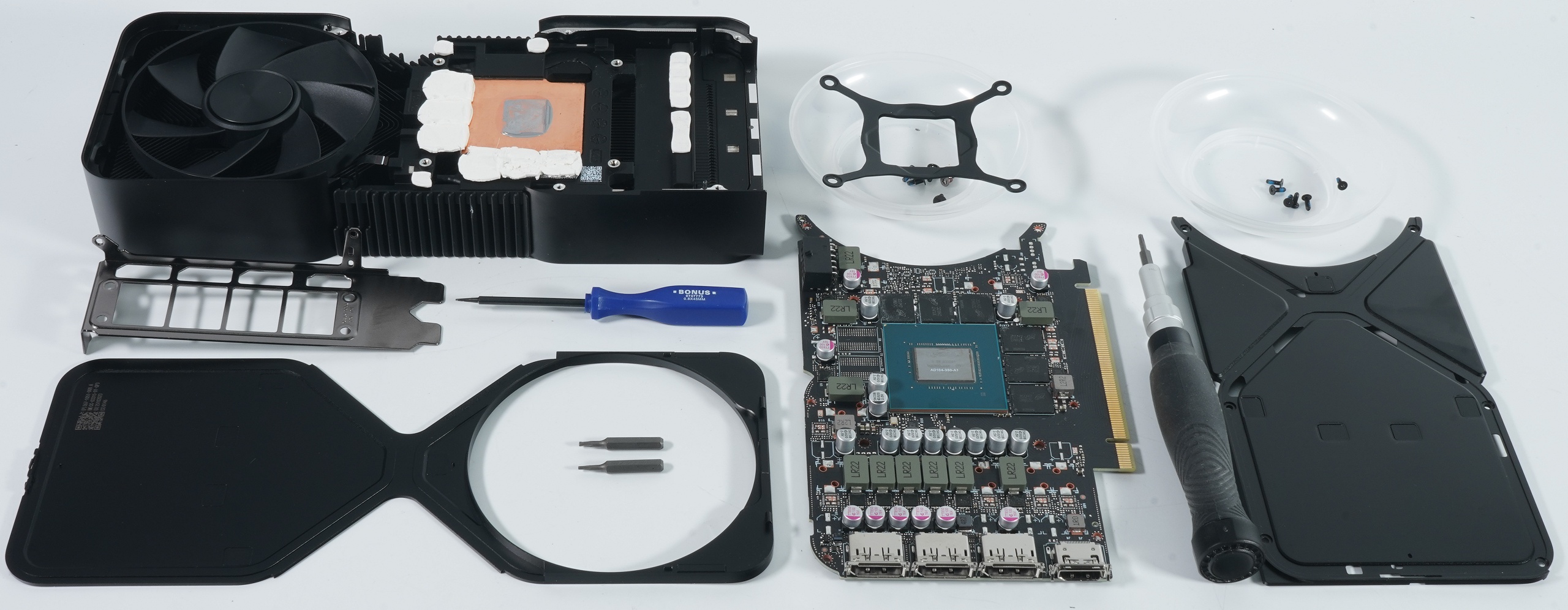
The rest is quickly explained. A solid copper heatsink is used instead of the usual vapor-chamber and a total of four heatpipes. But I’ll refer you to the next page, because this time there will also be a material analysis, which has provided a little surprise, at least for the pads. The pads used here are in the style of the RTX 3080, i.e. ultra-soft and easy to shape, but a little unusual. So please read on with excitement!
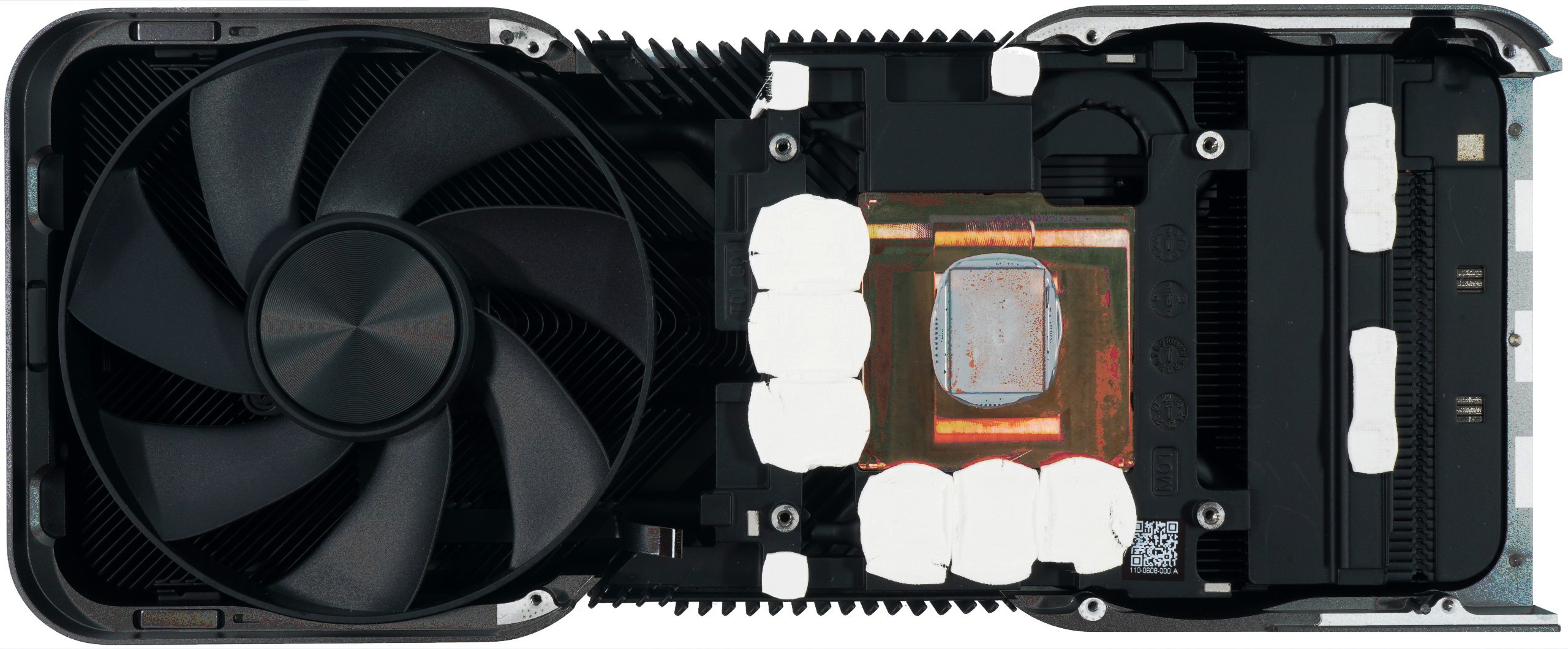
The inverse fan on the rear has a rotor diameter of 9 cm and uses seven rotor blades. The normally oriented fan on the front has a similar design. This explains the principle well enough, as it is still the same cooler.

- 1 - Introduction, technical Data and Features
- 2 - Test System and Equipment
- 3 - Teardown: PCB, Components and Cooler
- 4 - Material Analysis and a Surprise
- 5 - Gaming Performance FHD (1920 x 1080)
- 6 - Gaming-Performance WQHD (2560 x 1440)
- 7 - Gaming Performance Ultra-HD (3840 x 2160)
- 8 - Gaming Performance DLSS vs. FSR
- 9 - Gaming Performance Frame Generation
- 10 - Latencies in Detail
- 11 - Workstation Graphics and Rendering
- 12 - Power Consumption and Load Balancing
- 13 - Transients and PSU Recommendation
- 14 - Temperatures, Clock Rate and Infrared Analysis
- 15 - Fan Curves and Noise
- 16 - Summary and Conclusion


61 Antworten
Kommentar
Lade neue Kommentare
Veteran
Veteran
Veteran
Veteran
1
Veteran
Urgestein
Urgestein
1
Mitglied
Veteran
1
Mitglied
Mitglied
Veteran
Urgestein
Veteran
Urgestein
Alle Kommentare lesen unter igor´sLAB Community →