Today it’s getting super again. NVIDIA is officially launching the GeForce RTX 4070 Super in the form of the so-called MSRP cards. With a starting price of USD 599 or an RRP of EUR 659, the new Super-Susi is not that far off the street price of the RTX 4070 Non-Super, which starts at just under EUR 600. Today’s test will have to prove whether you will really notice the targeted 60 euro surcharge, but I can already spoil it: it will be really exciting!
And what does the customer do? Let’s look back: 9 months ago, NVIDIA released the RTX 4070 Non-Super as a mid-range card for an RRP of 659 euros, hoping to gain ground in this important segment. Then came AMD’s Radeon RX 7800XT and also wanted to score points on price, which pushed the price of the Non-Super down considerably. And now the GeForce RTX 4070 Super is entering the market with the same price recommendation as back then and still wants to do a lot better, i.e. faster. That’s exactly where my focus will be, because the rest has hardly changed since the first launch, even as far as the older generations are concerned.
For technical reasons, there is unfortunately no comparison with the RTX 3000 series today, but it was more important to me to first test all the new cards from NVIDIA and AMD with a new system, more suitable games and new drivers from scratch. The now second mainboard of the old system had unfortunately also given up the ghost after the first new benchmarks (certainly not unexpected after over 100 graphics card and CPU changes), but unfortunately a replacement could not be found so quickly. That’s why I switched to a private Core i9-13900K, which I could easily raise to KS level and thus also to the level of an i9-14900K. Sometimes binning pays off after all.
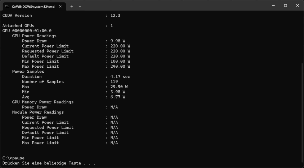
Today, I’m testing the NVIDIA GeForce RTX 4070 Super FE 12 GB in its as-delivered state, whereby it is representative of the entire 220-watt class of so-called MSRP cards, as the performance is identical. The fact that the manually achievable 240 watts takes you into the range of the OC cards that will be launched tomorrow is a nice feature of the FE card, but not the issue today. I’ll explain why I wouldn’t take advantage of this, at least without a mod, in the temperature measurements. And without spoiling anything in advance: you can also exceed the advertised 240 watts in the real stress test, which will also be a topic in due course.
Important foreword
Of course, as usual, there are many benchmarks, the comprehensive teardown, a very elaborate board, cooler and material analysis with some reverse engineering, as well as the analysis of the power consumption and load peaks including a suitable power supply recommendation. As I know that many colleagues will also repeat all the technical details and theory, which have already been presented in various snippets, I’ll save myself the trouble today and just briefly refer to the data already known. After all, you want to see real figures today and not PR fireworks. The specs will of course be coming soon.
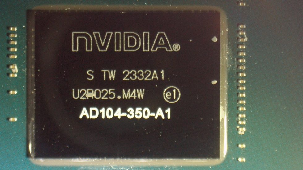
The Founders Edition of my press sample has a chip from calendar week 32 of 2023 in the form of the AD104-350-A1. And yes, it is a Bin-1 chip, i.e. the slightly better silicon from the many buckets.
The AD 104 and the new Ada architecture
The 294.5 mm² chip of the NVIDIA GeForce RTX 4070 Super is also manufactured in the TSMC 4N process and has the familiar 35.8 billion transistors. The AD104-350 has four graphic processing clusters (GPC) and 56 (instead of 46) new streaming multiprocessors (SM) with 7168 CUDA cores (instead of 5888), whose performance and energy efficiency have increased significantly compared to Ampere. In addition, there are 224 (formerly) 184 4th generation Tensor Cores and Optical Flow, which enables transformative AI technologies, including NVIDIA DLSS and the new frame rate multiplier NVIDIA DLSS 3.
The 56 (instead of 46) 3rd generation RT cores offer up to 2x ray tracing performance, while Shader Execution Reordering (SER) also improves ray tracing operations by a factor of two. In addition, there are a total of 23 Texture Processing Clusters (TPC), 184 Texture Units (TU) and 64 ROPs. The L2 cache has a total size of 48 MB and, 16 more than the GeForce RTX 4070 Non-Super and the card uses the familiar 12 GB GDDR6X with 10500 MHz clock rate on a rather narrow 192-bit interface, which corresponds to a data rate of 21 Gbps and a bandwidth of 504 GB/s. The AD104-350 of the GeForce RTX 4070 also offers only one NVDEC (decoder) instead of four and a single NVENC (encoder). The AV1 encoder is said to work up to 40% more efficiently than H.264.
The card still relies on a PCIe Gen. 4 interface and only for the external power connection with the 12VHPWR connector (12 4 pin) on an element of the PCIe Gen. 5 specification. The TGP is 220 watts and, depending on the board partner, can also be increased to up to 255 watts (which is rather pointless because the voltage is limited at some point anyway).
| RTX 4080 Super | RTX 4080 | RTX 4070 Ti Super | RTX 4070 Ti | RTX 4070 Super | RTX 4070 | |
|---|---|---|---|---|---|---|
| GPU | AD103 | AD104 | ||||
| Transistors | 45.9 billion | 35.8 billion | ||||
| The size |
379 mm² | 295 mm² | ||||
| SM | 80 | 76 | 66 | 60 | 56 | 46 |
| FP32-ALUs | 10.240 | 9.728 | 8.448 | 7.680 | 7.168 | 5.888 |
| RT Cores | 80, 3rd Gen | 76, 3rd Gen | 66, 3rd Gen | 60, 3rd Gen | 56, 3rd Gen | 46, 3rd Gen |
| Tensor Cores | 320, 4th Gen | 304, 4th Gen | 264, 4th Gen | 240, 4th Gen | 224, 4th Gen | 184, 4th Gen |
| Base Clock | tbc | 2.210 MHz | tbc | 2.310 MHz | 1.980 MHz | 1.920 MHz |
| Boost Clock | tbc | 2.510 MHz | tbc | 2.610 MHz | 2.475 MHz | 2.475 MHz |
| FP32-Perf | 52 TFLOPS | 48.8 TFLOPS | 44 TFLOPS | 40.1 TFLOPS | 35 TFLOPS | 29.1 TFLOPS |
| L2 cache | 64 MB | 48 MB | 32 MB | |||
| Memory | 16 GB GDDR6X | 12 GB GDDR6X | ||||
| Throughput | 23 Gbps | 22.4 Gbps | 21 Gbps | |||
| Interface | 256 bit | 192 bits | ||||
| Bandwidth | 736 GB/s | 717 GB/s | 672 GB/s | 504 GB/s | ||
| Video engine | 2 × NVENC (8th Gen) 1 × NVDEC (5th Gen) |
1 × NVENC (8th Gen) 1 × NVDEC (5th Gen) |
||||
| TDP | 320 watts | 285 watts | 220 watts | 200 watts | ||
| RRP (DE) | 1.109 Euro | 1.329 Euro | 889 Euro | 899 Euro | 659 Euro | 659 Euro |
The NVIDIA GeForce RTX 4070 FE 12 GB in detail
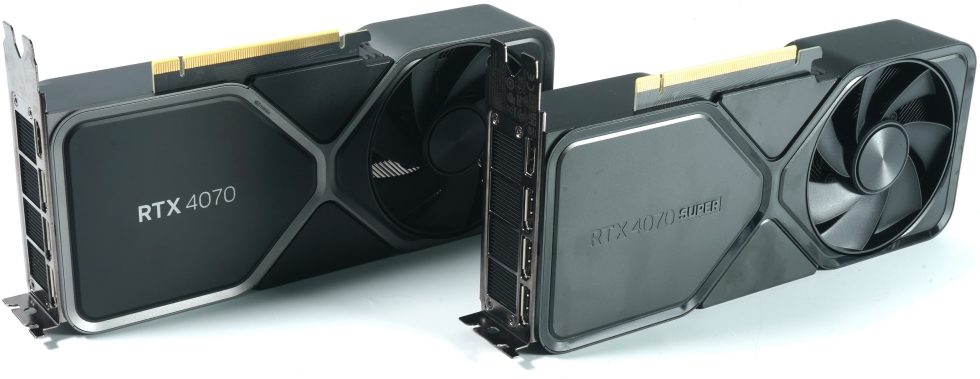
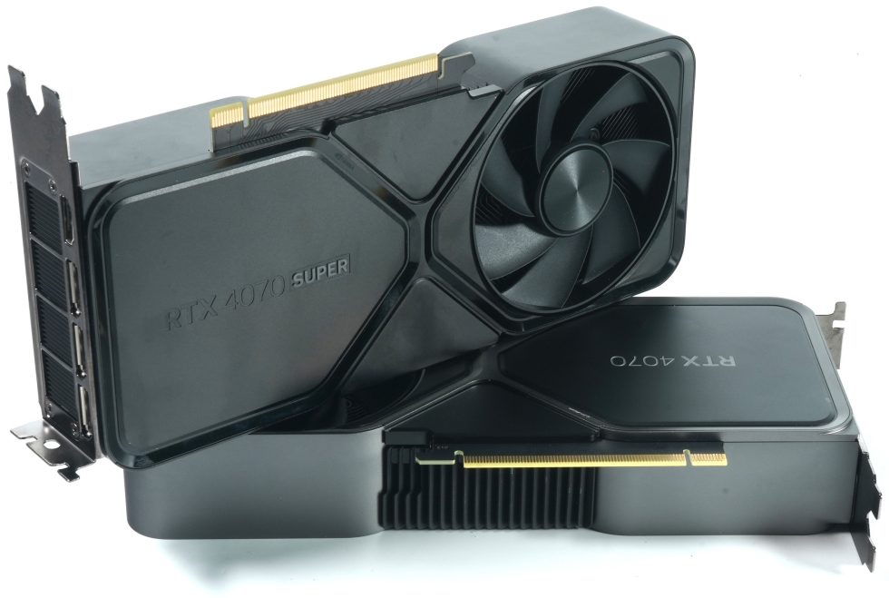
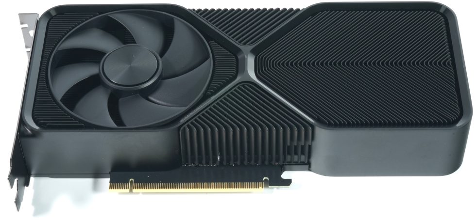
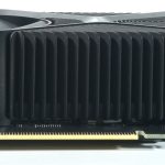
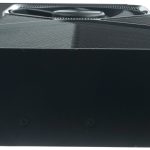
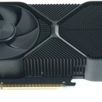
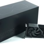
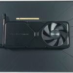
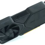
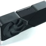
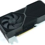
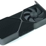
The card weighs just 1022 grams, which is 2 grams more than the RTX 4070 Non-Super. The length of 24.5 cm is moderate and the height of 10.5 cm is normal. There’s no need for a large case, even if you have to use the great 12VHPWR adapter, which gets by with 2x 6 2-pin PCIe outputs. The installation depth is 3.8 cm plus the 5 mm for the backplate attachment on the rear. This makes it a true dual-slot card and just as big as the non-super. This time, however, all surfaces have been nicely blackened: Black Beauty incoming…
The light metal frame is familiar and the design language of the fan, cover and slot bracket is not new either. The only difference is that everything looks a lot smaller. NVIDIA uses a single BIOS and if you want to overclock, you have to use a suitable tool. As usual, the feel is of high quality, the cards have a collector’s value and look pleasantly timeless. Incidentally, there is also an exciting material analysis waiting for you.
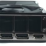
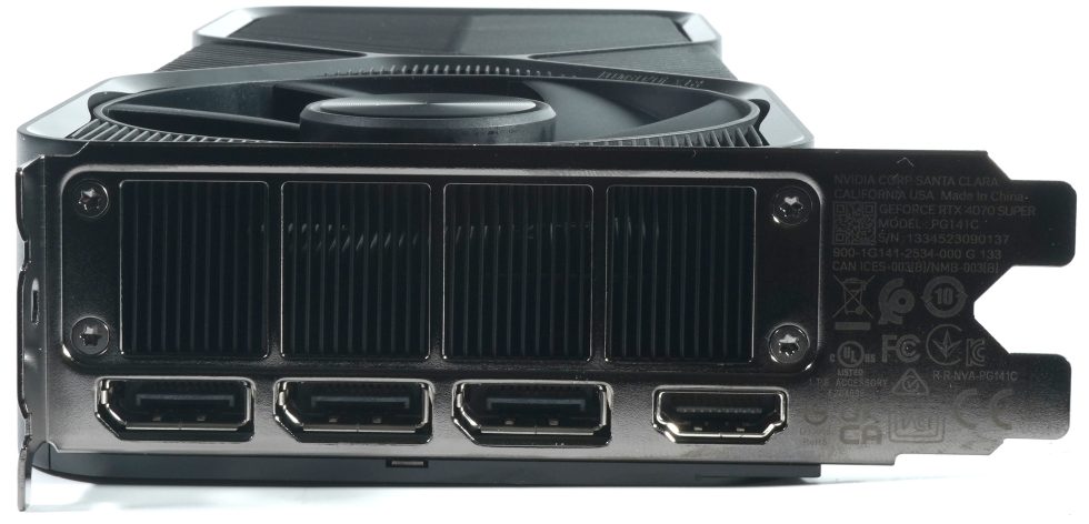
You can not only plug power into the card, but also video connections. There are four of them, to be precise: three DisplayPort 1.4a and one HDMI 2.1a. This is a shame, especially for DisplayPort, when it comes to the new specifications. A missed opportunity, unfortunately. And with HDMI, you have to play around with the compression from 4K onwards if you want to go above 120 Hz.
That’s this first page done and we’re slowly getting ready for the test.
- 1 - Introduction, technical Data and Features
- 2 - Test System and Equipment
- 3 - Teardown: PCB, Components and Cooler
- 4 - Material Analysis and a Surprise
- 5 - Gaming Performance FHD (1920 x 1080)
- 6 - Gaming-Performance WQHD (2560 x 1440)
- 7 - Gaming Performance Ultra-HD (3840 x 2160)
- 8 - Gaming Performance DLSS vs. FSR
- 9 - Gaming Performance Frame Generation
- 10 - Latencies in Detail
- 11 - Workstation Graphics and Rendering
- 12 - Power Consumption and Load Balancing
- 13 - Transients and PSU Recommendation
- 14 - Temperatures, Clock Rate and Infrared Analysis
- 15 - Fan Curves and Noise
- 16 - Summary and Conclusion






61 Antworten
Kommentar
Lade neue Kommentare
Veteran
Urgestein
Veteran
Veteran
1
Veteran
Urgestein
Urgestein
1
Mitglied
Urgestein
1
Mitglied
Mitglied
Veteran
Urgestein
Veteran
Urgestein
Alle Kommentare lesen unter igor´sLAB Community →