


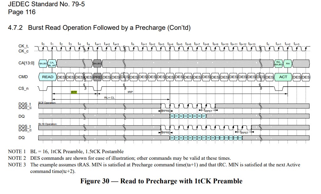
tRTP / tRDPRE explained
The timing tRTP as it is called by JEDEC does not actually exist in Intel memory controllers. Instead, there is the tRDPRE timing, which is effectively just another abbreviation for the description of the same function. After a read operation, a row and the associated bank and bank group must be deactivated again and precharged in the process so that it can be reactivated and read again later. This process is called Precharge and is controlled by the timing tRP. tRTP or tRDPRE now defines how much time elapses between the end of the read operation and deactivation and charging. Again, the principle is similar to a “breather” after the read operation before the Bank Group is returned to its initial state.
tRTP is defined in the official JEDEC document for DDR5 so that the minimum supported value is the maximum of 12 nCK (number of clock cycles) or 7.5 ns. Of course, the clock rate is then relevant here to determine whether 12 clock cycles are longer than 7.5 ns. For DDR5-4800, the actual clock rate is known to be 2400 MHz – DDR = Double Data Rate. 1 nCK thus corresponds to 1 s / 24000000 or also 4.16 e ^ -10 s. 12 times that are accordingly 5 e^-9 s or 5 ns. The maximum of 12 nCK and 7.5 ns is therefore 7.5 ns with DDR5-4800.
![]()
The other way around, this can also be converted back into clock cycles to determine the minimum timing value that is supported according to JEDEC. To do this, we simply divide the 7.5 ns by the duration of a single clock cycle and round this to the nearest integer. 7.5 e^-9 s / 4.16 e^-10 s = 18.02. Thus, the lowest value for tRTP supported according to JEDEC for DDR5-4800 is actually 19 and not 12.
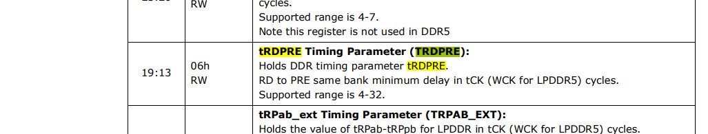
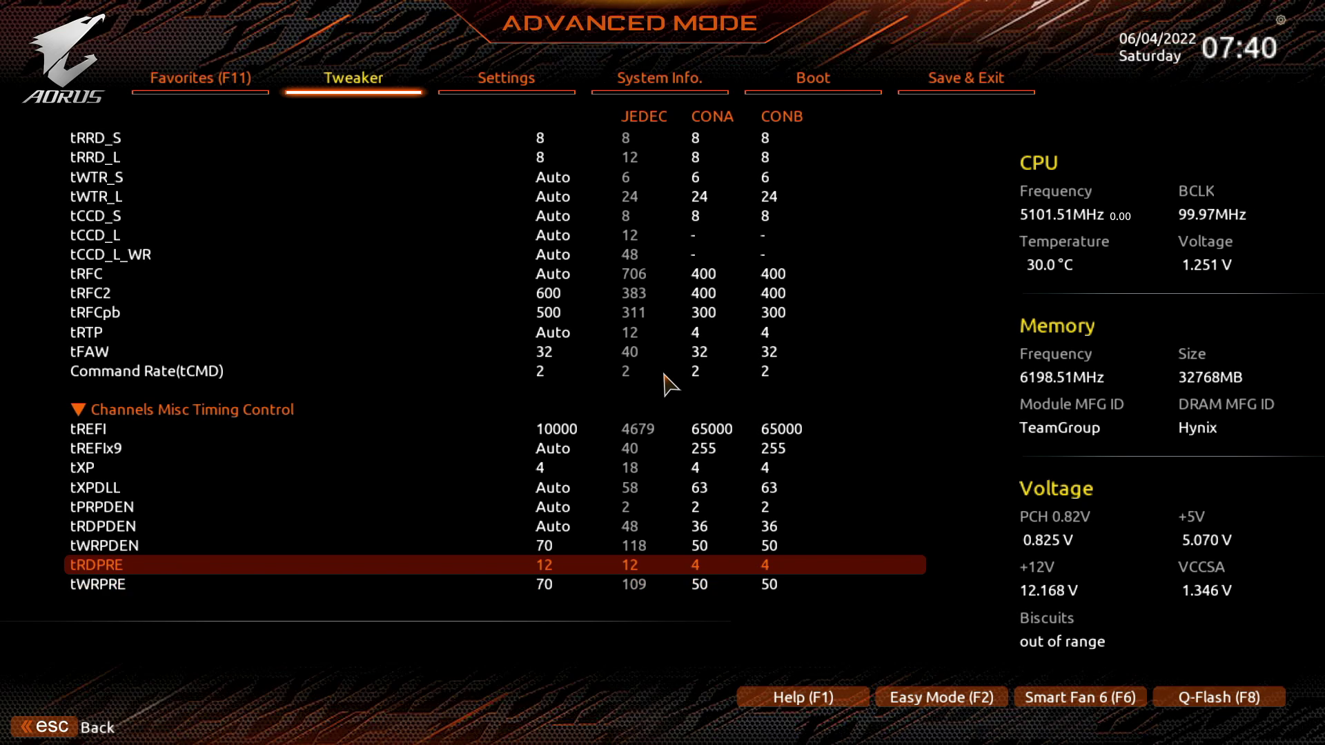
What does Intel have to say about this? Well, nothing, because strictly speaking, Intel does not specify the timing at all. Instead, the other timing tRDPRE effectively takes over this function. Accordingly, you can leave tRTP on Auto in the BIOS of most motherboards and control the value via tRDPRE instead, which allows lower values in some cases, but that’s just a side note. Intel does not specify any effective time periods in their documentation, but only a number of clock cycles. In the case of tRDPRE, the supported range is 4 – 32.
If we convert this back to nanoseconds for DDR4-4800 for reference, we end up with 1.67 ns and 13.312 ns, respectively, and thus with the minimum well below the JEDEC standard. By the way, JEDEC does not specify a maximum at all. To summarize this again for DDR5-4800: Intel specifies a minimum of 1.67 ns, while JEDEC defines a minimum of 7.5 ns. This is a stark difference that only gets bigger with increasing clock rates, since the JEDEC value is fixed, but the Intel value shrinks inversely proportional with the clock rate. But what now brings the most performance? We have also tested this with several gradations for the timing value.


Bisher keine Kommentare
Kommentar
Lade neue Kommentare
Artikel-Butler
Alle Kommentare lesen unter igor´sLAB Community →