


Teardown and PCB analysis
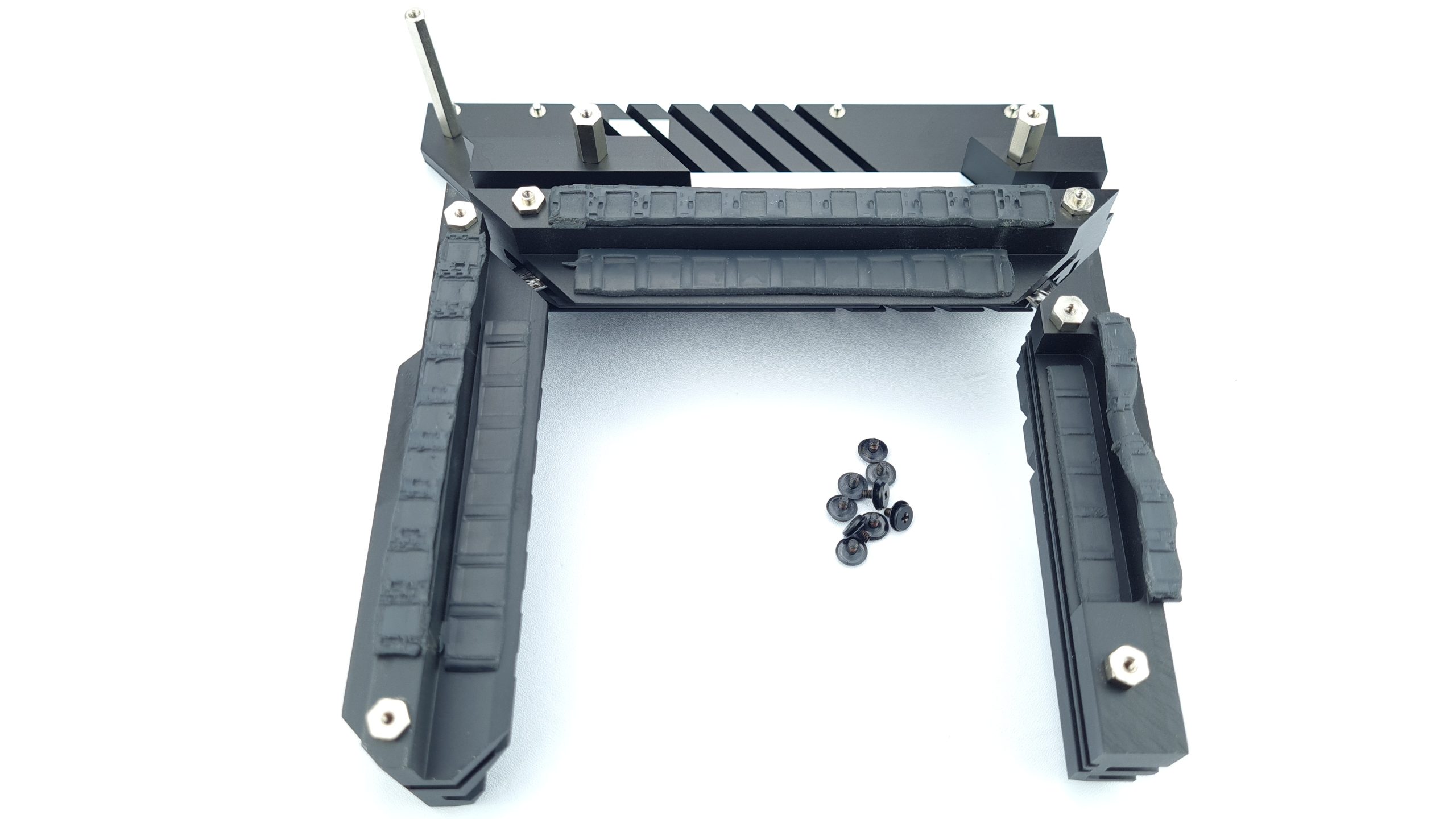
To remove the M.2 cooler, just remove 5 Phillips screws on the front. The two slots with a length of 80 mm each and the tool-free mounting mechanism are revealed underneath. By the way, next to the Maximus Z690 Apex lettering you can also find the revision number R1.02, which is the same on both of my boards. Of course, I also don’t want to leave the shorter PCI Express slots unmentioned, each with 3.0 standard connected via the chipset and with x1 or x4 length, whereby the latter can also accept longer cards.
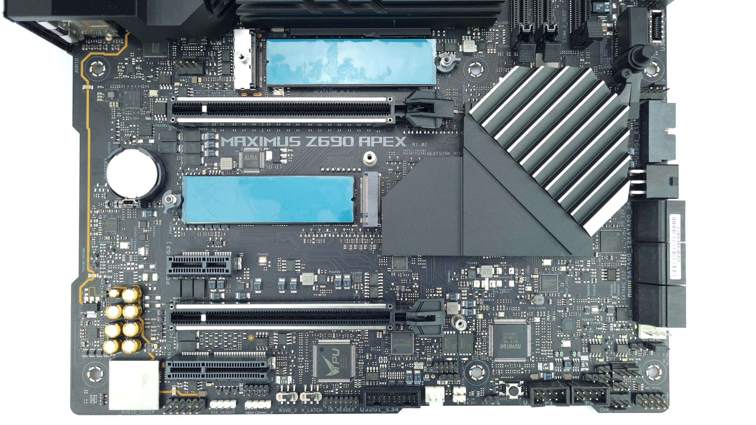
We can also see the “Q-Release” button quite well from here, which is effectively a steel cable diverted over pulleys, making it easier to open the upper PCI-Express slot closure. Especially with the massive M.2 cooler right next door, this new feature is very welcome.
By removing 9 more Phillips screws, this time from the back, the power supply cooler can also be removed relatively stress-free. This consists of 3 aluminum blocks that are thermally connected with a heat pipe. Asus has also paid attention to the color choice for the thermal pads and remains inconspicuously black. As we can already see here, the power supply actually extends over 3 sides of the base, so the waste heat from the components is also better distributed.
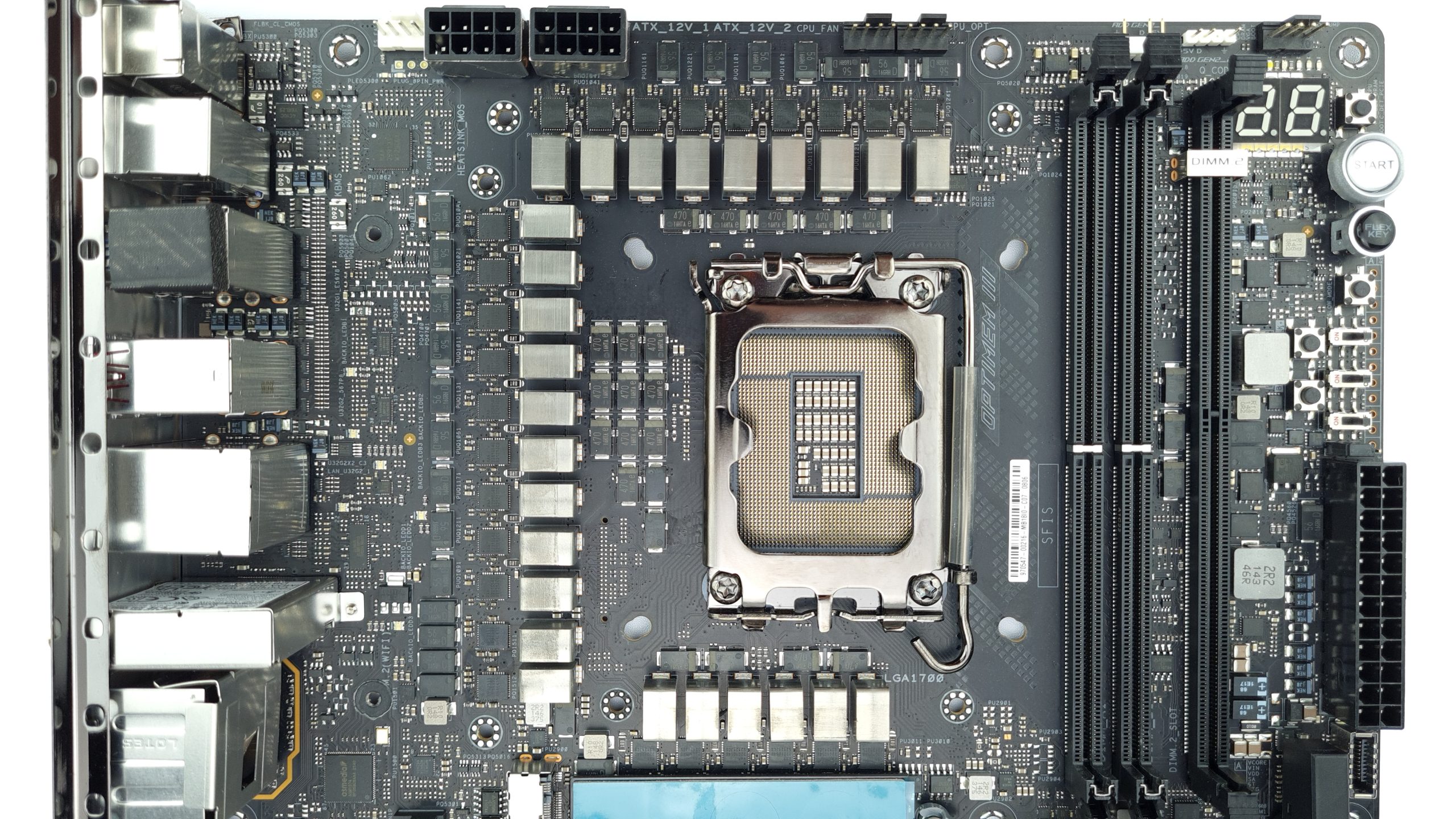
A total of 24 pairs of powerstage and inductor provide the CPU voltage around the socket, whereby these are teamed so that there are 12 real phases. In the lower left corner there are two extra phases for the 1.8V AUX rail of the integrated voltage converter of the CPU (FIVR). There is no power supply for the CPU’s integrated graphics unit, so it cannot be used. Resourceful readers will surely have noticed this with the lack of display outputs on the IO.
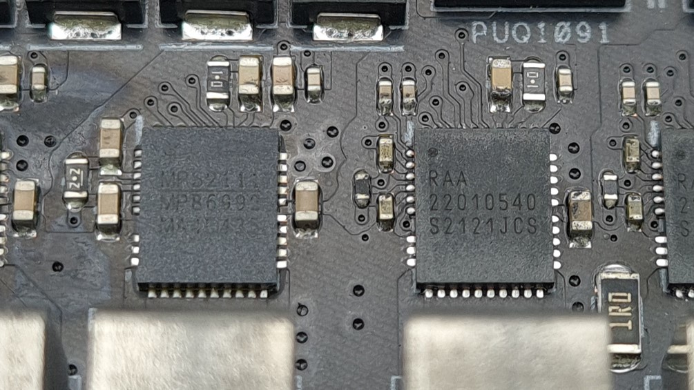
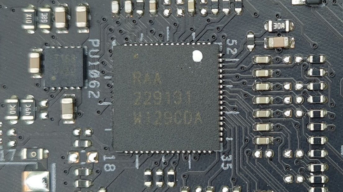
The voltage transformers for Vcore are RAA 22010540 Smart Power Stages from Renesas, specified with a rated current of 105 amps. These are controlled by an RAA 229131 20-phase PWM controller, also from Renesas. AUX power is provided by two MP86992 Smart Power Stages from Monolithic Power Systems, each rated at 70 amps.
Asus also relies almost entirely on SMD aluminum-polymer capacitors for the filtering of the power supply, both for the input and output side, whereby even 3-terminal components with 470 uF are used for Vcore smoothing, with theoretically even faster ESL and ESR values. Asus relies entirely on multilayer ceramic capacitors in the socket.
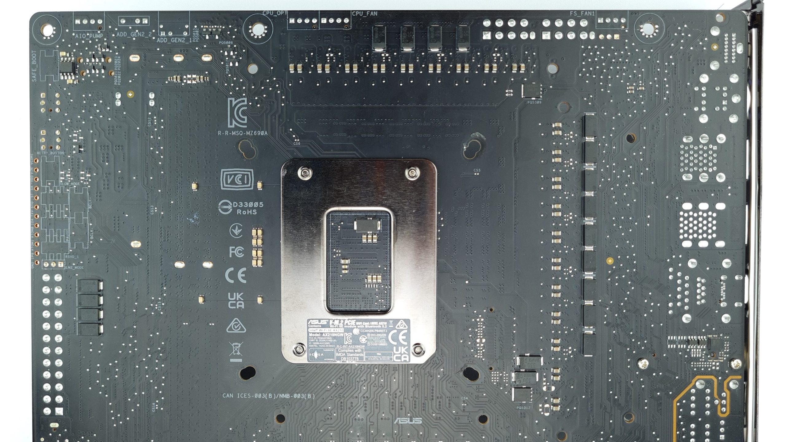
Asus also installs numerous capacitors on the back for voltage smoothing of the VRMs. Only the base looks a bit empty here, although the first impression is deceiving. Besides a few more MLCCs, there is even an SP cap, and anything more would probably just be overkill considering the quality of the installed components. In addition to the 78 mm holes for the LGA1700 socket, Asus also integrates 75 mm holes, which should be a simplification especially for extreme overclockers with existing LN2 pots. Unfortunately, there is no hole in the back of the base for a temperature sensor.
The power supply for the CPU couldn’t be more lush and so exactly this component selection also finds its way onto the even more expensive motherboards of the Maximus Z690 motherboard series, possibly only with an additional iGPU rail. At least on paper, there is almost no motherboard that can still keep up with the Z690 Apex in terms of CPU voltage regulation. So, good omens for overclocking for LGA1700 CPUs on a record hunt. By the way, the board is an 8-layer design, as an Asus contact confirmed to us.


43 Antworten
Kommentar
Lade neue Kommentare
Veteran
Mitglied
Veteran
Veteran
Veteran
Mitglied
Veteran
Veteran
Urgestein
1
Veteran
Veteran
Veteran
Veteran
1
Mitglied
Urgestein
1
Mitglied
Alle Kommentare lesen unter igor´sLAB Community →