


What do you do to raise awareness of a new product as a manufacturer? You simply split the launch of such a GeForce RTX 4070 12 GB and first release the cards that are also offered at the MSRP. So beautiful, so unexciting, because in the end all these cards are somehow the same. Except for one, because it is much more equal than the others. And this is NVIDIA’s own Founders Edition. However, while the power limit of all so-called “MSRP cards” is capped at 200 watts, the Founders Edition allows 20 watts more and is thus actually a disguised OC card that only has to be manually set to this socket.
And what does the customer do? For an MSRP of 659 Euros, NVIDIA lets the entry-level cards off the leash today and hopes to gain ground in the all-important mid-range. In the end, I can already spoil that the performance is more like that of a GeForce RTX 3080 FE 10 GB, except that there is even 2 GB more memory available here. Based on the technical data, the GeForce RTX 3080 10GB would probably have more of an advantage, but paper is patient and the reality is much more differentiated. Yes, the price is not really the groundbreaking special offer now, but it could have been worse. And as long as the direct competitor does not have anything new to offer in this class, NVIDIA will have the sole authority in terms of price.
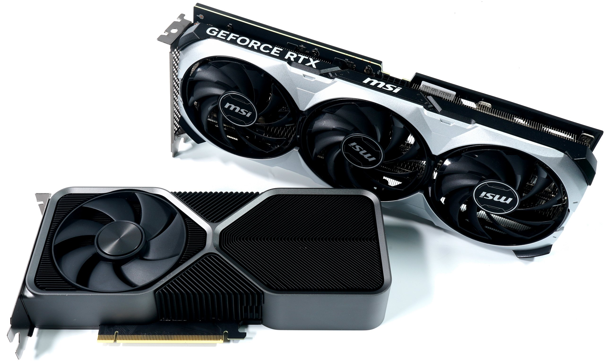
I compared the NVIDIA GeForce RTX 4070 FE with the MSI RTX 4070 Ventus and the PNY RTX 4070 12 GB before in terms of performance, and the difference is at or even below one percent, which passes for measurement inaccuracy and chip lottery, with the MSI card having the worse cooler than the FE. The PNY card is a bit of everything and lies dutifully in between. So for performance today, I’m going to do something other than juxtapose all three cards in an accounting-correct way. Nobody is interested in bars of the same length anyway. I will then present the single cards step by step in detail, because there are definitely differences in the technical implementation, the coolers and the optics. But everything in its own time. So there will be several more individual reviews, don’t worry. Only for today it was all just too much.
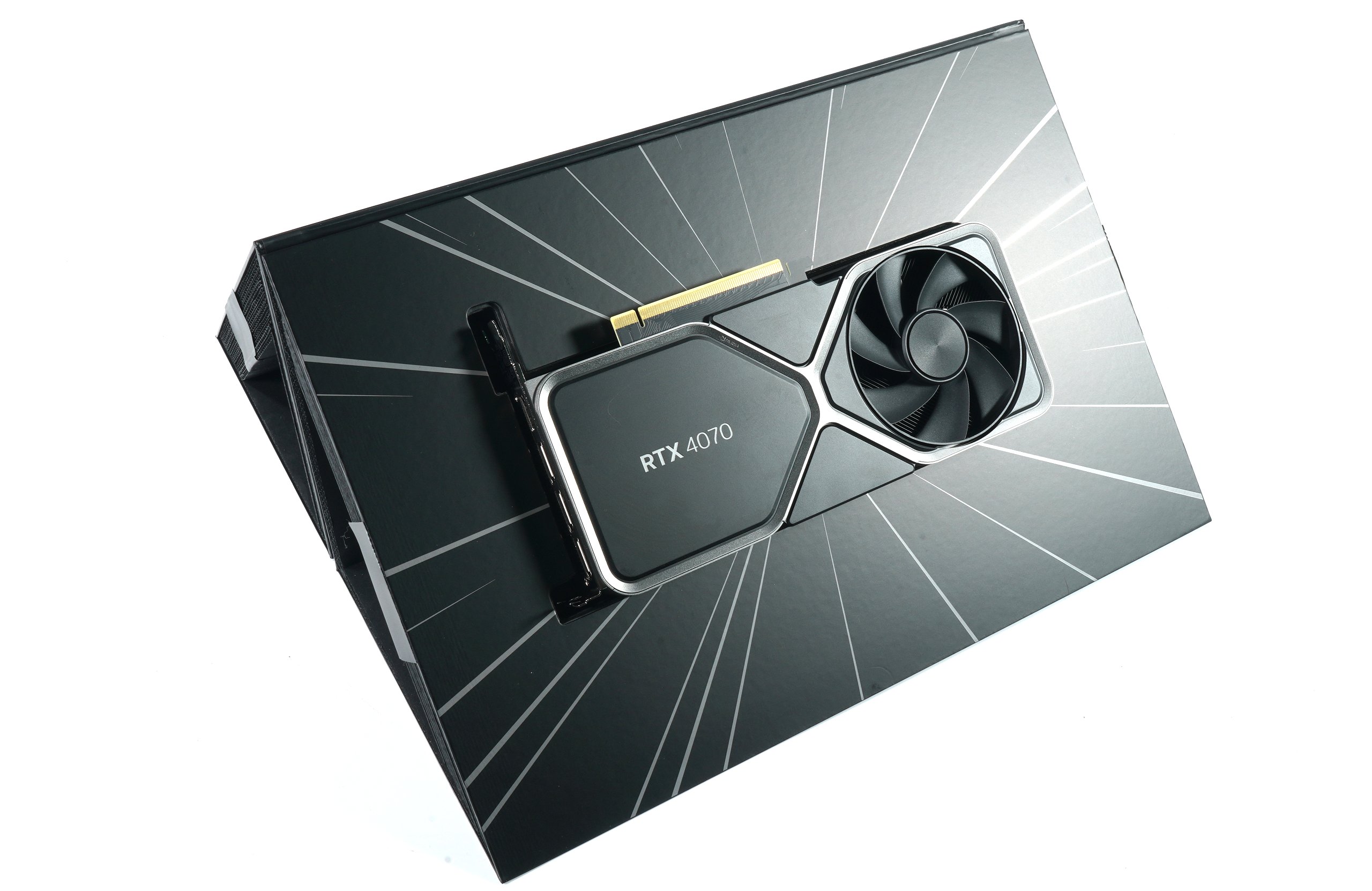
Instead, I’m testing the NVIDIA GeForce RTX 4070 FE 12 GB out of the box today, where it represents the entire 200 watt class of so-called MSRP cards, because the performance is identical. And, of course, there’s the topping of the run with the 220 watts as the maximum power limit, where I increased the clock by another 150 MHz. It’s not my fault that this is in the range of OC cards that will only be launched tomorrow. The card can and that’s why I’m showing it. And without spoiling anything forbidden: I never needed more than 215 watts, not even at the clock limit. That’s why I can sleep quite well the night before the launch and save myself a double.
Important preface
Of course, there are many benchmarks as usual, the comprehensive teardown, a very elaborate board and cooler analysis with some reverse engineering, as well as the analysis of the power consumption and the load peaks including a suitable power supply recommendation. Since I know that many colleagues will also repeat all the technical details including theory, which have already been presented in various tidbits, I’ll spare myself that today on a large scale and only briefly refer to the already known data. After all, you want to see real figures today and not PR fireworks. Of course, the specs are coming later on this page.
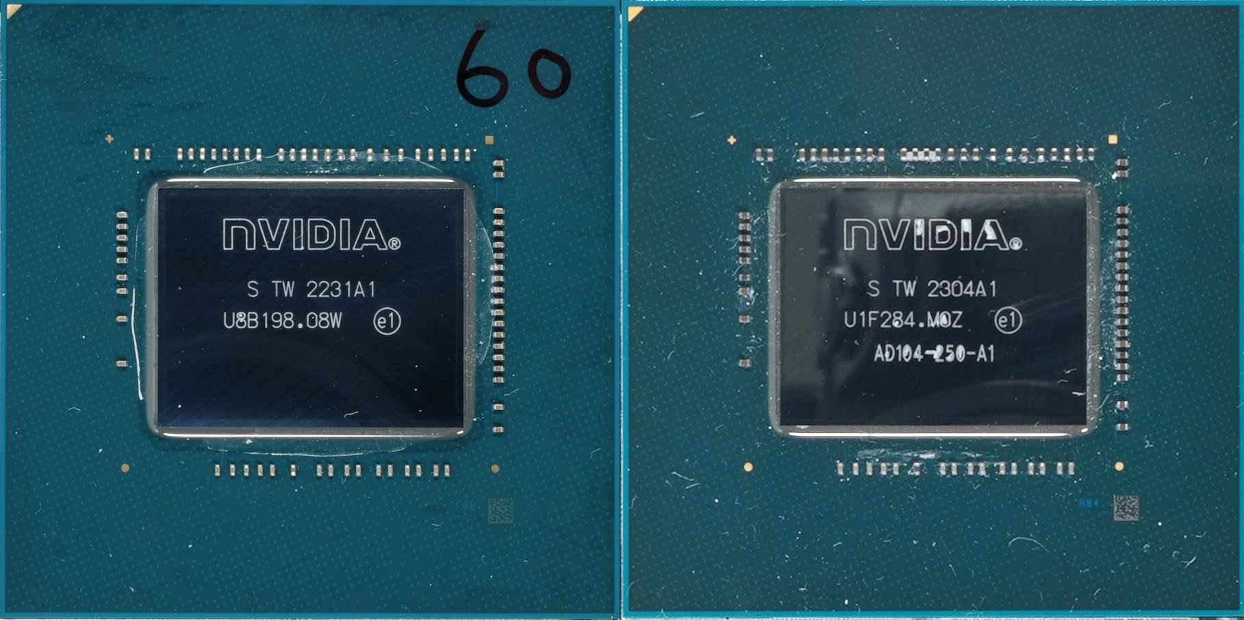
However, I will go into more detail about all the metrics including DLSS 3 and, at the appropriate places, various teasers up to the latencies, about which a colleague (Fritz Hunter) is preparing a larger special on Friday. Since the effort here is higher, this of course takes a little more time. Thus, the 4070 week would be complete. And there is a small difference in the chips as well. While the Founders Edition of my press sample has a chip without a type designation from week 31 of 2022 including a hand-painted number, the AIC cards rely on newer chips like the MSI Ventus with a completely labeled AD104-250 from week 4 in 2023.
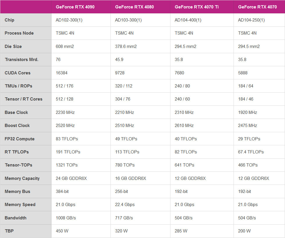
The AD 104 and the new Ada architecture
The 294.5 mm² chip of the NVIDIA GeForce RTX 4070 is also manufactured in the TSMC 4N process and has 35.8 billion transistors. The AD104-250 still has four Graphic Processing Clusters (GPC) and 46 new Streaming Multiprocessors (SM) with 5888 CUDA cores, whose performance and energy efficiency have increased significantly compared to Ampere. In addition, there are 184 tensor cores of the 4th generation. Generation and Optical Flow, enabling transformative AI technologies including NVIDIA DLSS and the new NVIDIA DLSS 3 frame rate multiplier.
The 46 RT cores of the 3rd generation The new generation offers up to 2x ray tracing performance, Shader Execution Reordering (SER) improves ray tracing operations by a factor of two. In addition, there are a total of 23 Texture Processing Clusters (TPC), 184 Texture Units (TU) and 64 ROPs. The L2 cache is 36864 KB in total and the card, like the GeForce RTX 4070 Ti, uses the familiar 12 GB GDDR6X clocked at 10500 MHz on a rather narrow 192-bit interface, which corresponds to a data rate of 21 Gbps and a bandwidth of 504 GB/s. The AD104-250 of the GeForce RTX 4070 only offers one NVDEC (decoder) instead of four and a single NVENC (encoder). The AV1 encoder is said to be up to 40% more efficient than H.264.

The changes to all three core types can be summarized quite simply:
- Programmable Shader: Ada’s SM includes an important new technology called Shader Execution Reordering (SER) that reorders work on the fly, providing a 2x speedup for ray tracing. SER is as big an innovation as the out-of-order design for CPUs was at the time. 83 shader TFLOPS are quite a statement
- Tensor Cores of the 4. Generation: The new Tensor Core in Ada includes the NVIDIA Hopper FP8 Transformer Engine, which delivers over 1.3 petaFLOPS for AI inference workloads in the RTX 4090. Compared to FP16, FP8 halves data storage requirements and doubles AI performance. The GeForce RTX 4090 thus offers more than twice the total Tensor Core processing power of the RTX 3090 Ti.
- RT Core of the 3. Generation: A new opacity micromap engine accelerates ray tracing of alpha-checked geometries by a factor of 2. Add to this a new micro-mesh engine that handles all the geometric richness without further BVH creation and storage costs. Triangulation throughput is 191 RT-TFLOPS, compared to Ampere’s 78 RTTFLOPS.
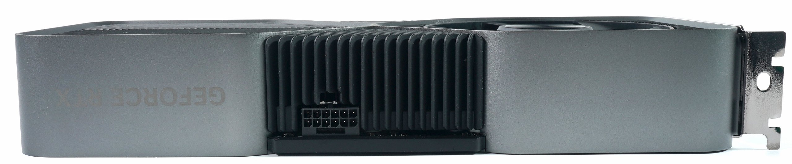
The card still relies on a PCIe Gen. 4 interface and only for the external power connection with the 12VHPWR connector (12+4 pin) on an element of the PCIe Gen. 5 specification. The TGP is 200 (220) watts and can also be raised up to 240 watts, depending on the board partner (which is rather pointless because the voltage limits at some point anyway).
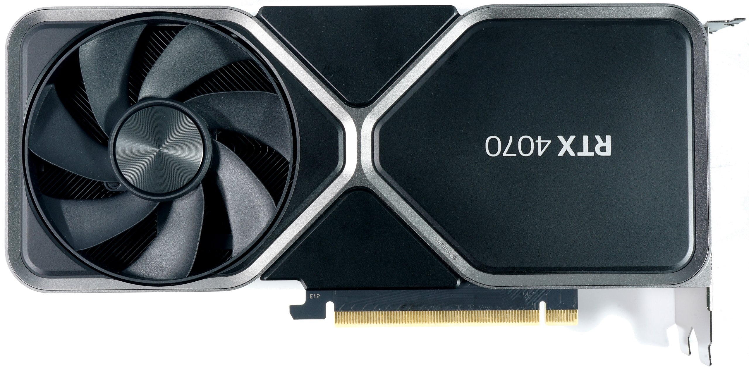
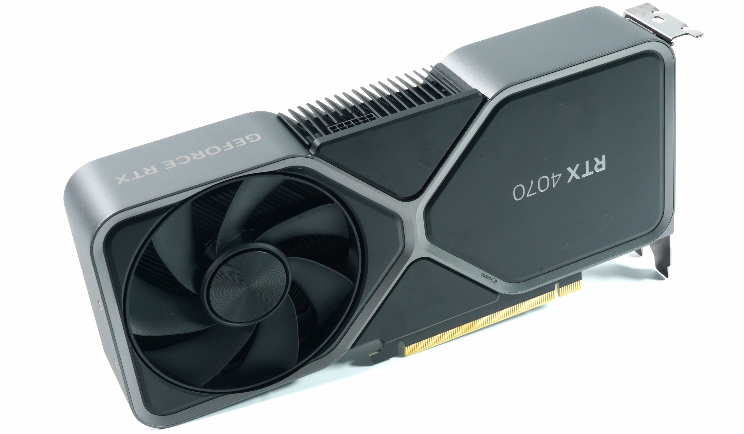
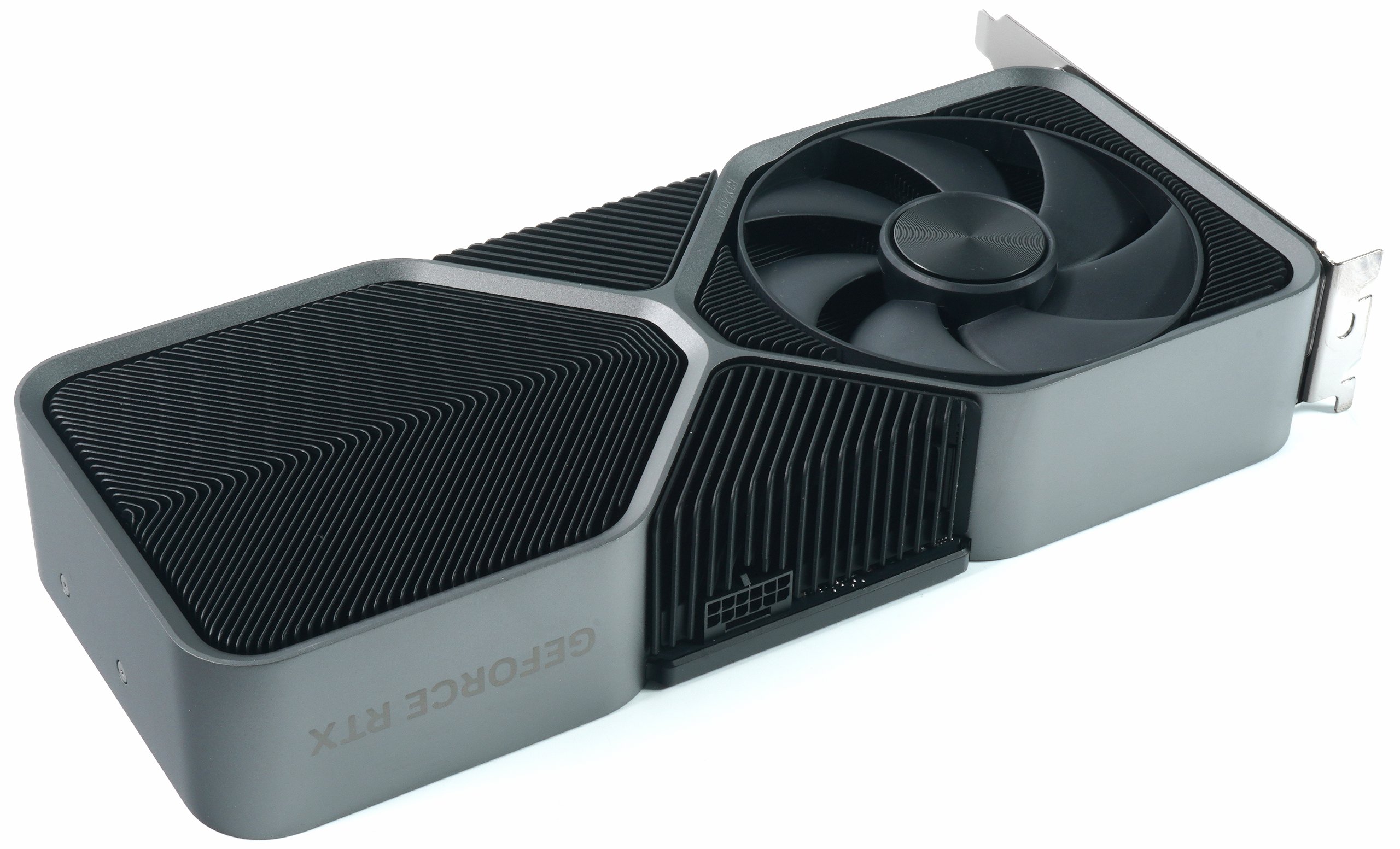
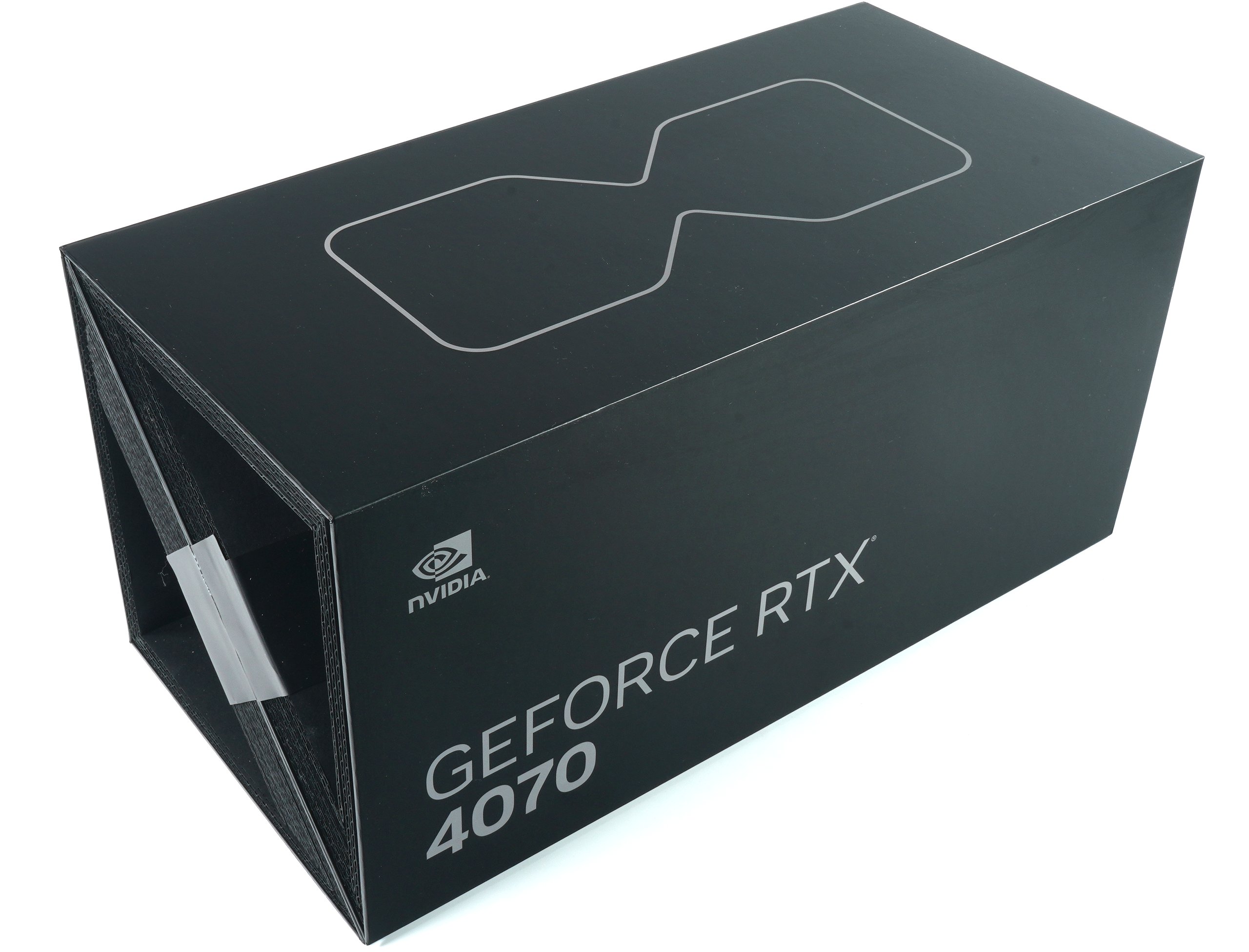
The NVIDIA GeForce RTX 4070 FE 12 GB in detail
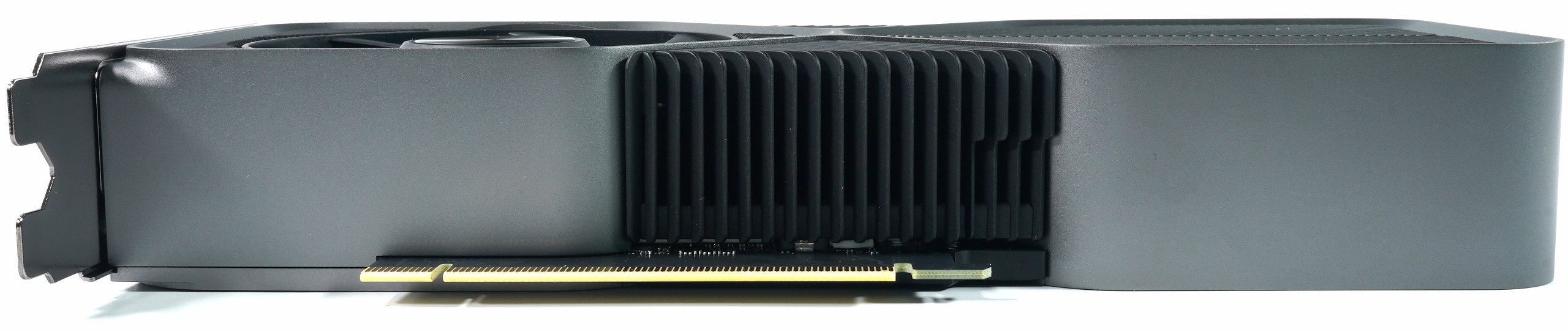
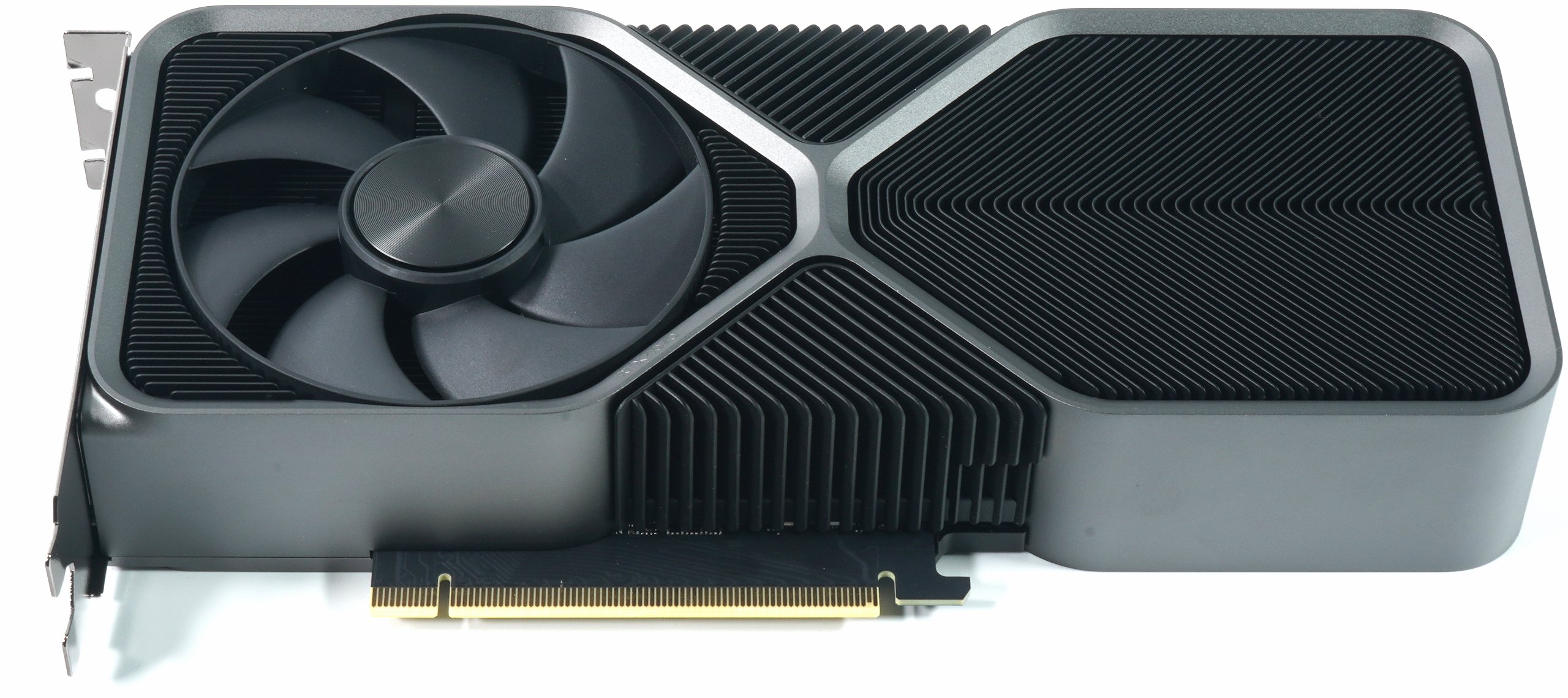
The card only weighs 1020 grams. The length of 24.5 cm is moderate and the height of 10.5 cm is on the normal size. There you don’t need a trum of housing, even if you have to use the great 12VHPWR adapter, but it gets by with 2x 6+2-pin. The installation depth is 3.8 cm plus the 5 mm for the backplate attachment on the rear. This makes it a true dual-slot card.
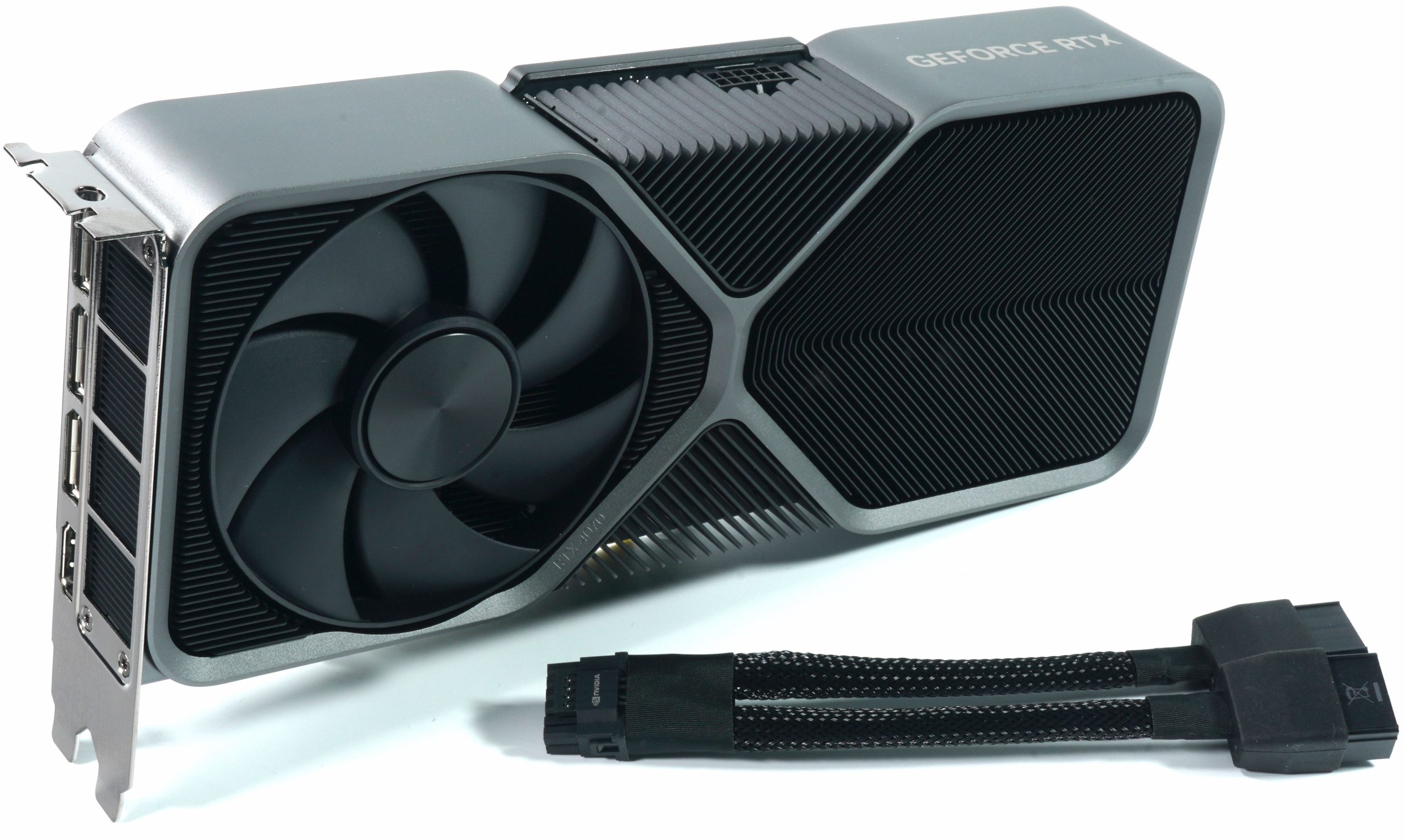
The light metal frame is well-known and the design language of the fan, cover and slot bezel is not new either. Except that everything looks abundantly shrunk. NVIDIA uses a single BIOS and those who want to overclock have to use a suitable tool. The feel is, as usual, high-quality, the cards definitely have collector’s value and appear pleasantly timeless.
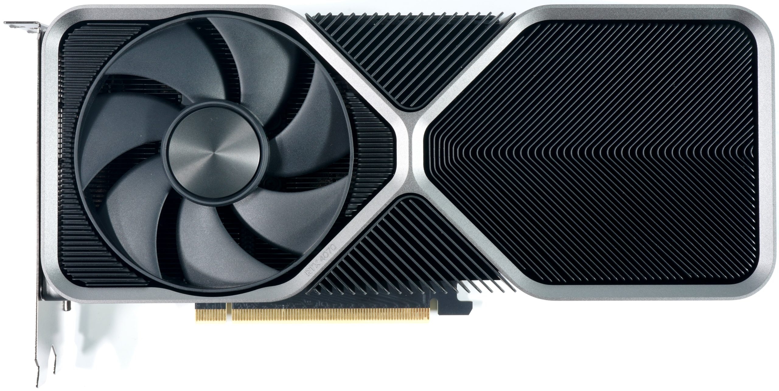
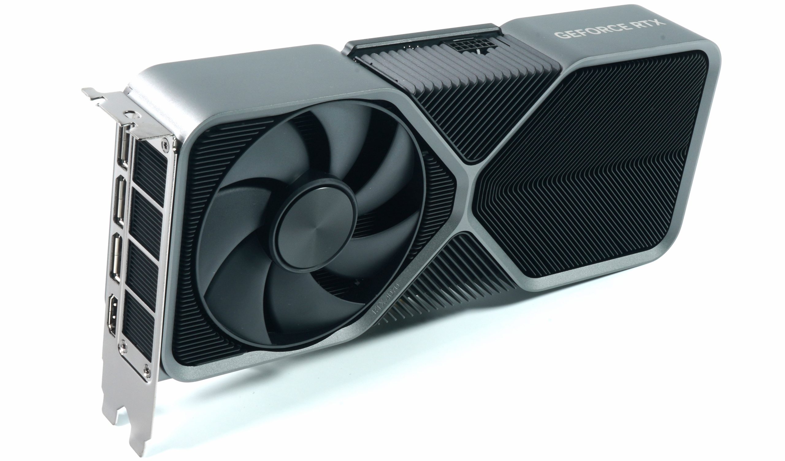
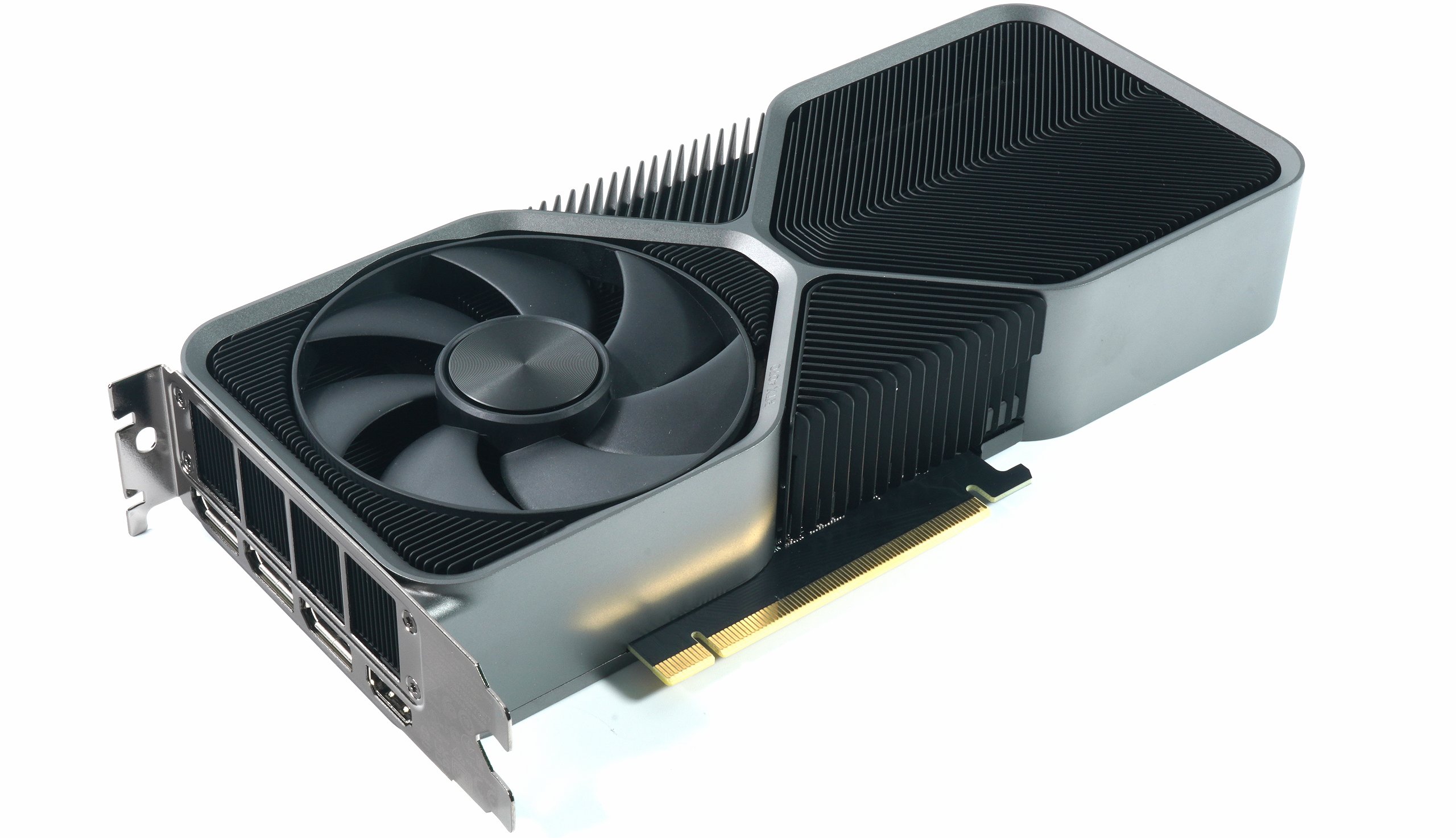
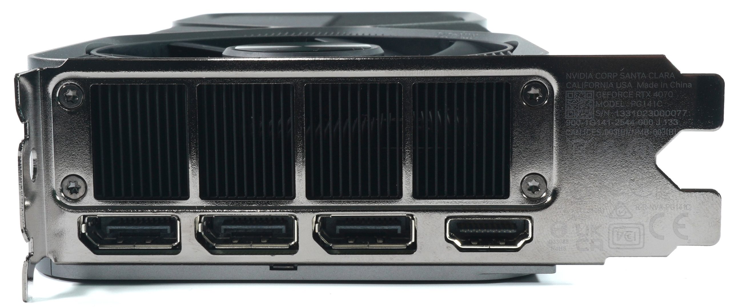
But you can not only put power into the card, but also video connections. There are four of them, to be quite precise, as there are: three times DisplayPort 1.4a and once HDMI 2.1a. That is especially a pity for the DisplayPort when it comes to the new specifications. Opportunity missed, unfortunately. And with HDMI, you have to trick with the compression from 4K onwards if you want it to go above 120 Hz.
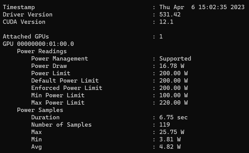
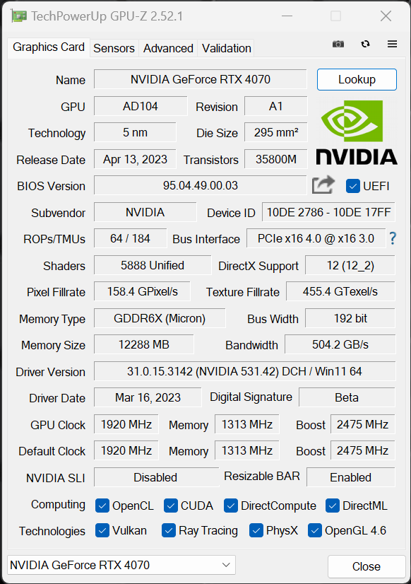
The screenshot from GPU-Z shows us default settings of the RTX 4070, which are identical for all 200-Watt cards:
With this, the first page is finished and we are slowly preparing for the test.

- 1 - Introduction, Specs and Unboxing
- 2 - Test system, equipment and methods
- 3 - Teardown: PCB, components and cooler
- 4 - Gaming Performance Full HD (1920 x 1080)
- 5 - Summe Gaming-Performance WQHD (2560 x 1440)
- 6 - Gaming Performance Ultra HD (3840 x 2160)
- 7 - Gaming Performance DLSS vs. FSR
- 8 - Latency and DLSS 3.0
- 9 - Workstation and rendering
- 10 - Power consumption and PEG loads
- 11 - Transients, cutting and PSU recommendation
- 12 - Clock rate and OC, temperatures and thermal imaging
- 13 - Fan speed and noise level
- 14 - Summary and conclusion


258 Antworten
Kommentar
Lade neue Kommentare
Moderator
1
Urgestein
Neuling
Urgestein
Neuling
1
Veteran
Neuling
Urgestein
Urgestein
Veteran
Mitglied
Mitglied
Veteran
Urgestein
Urgestein
Urgestein
Mitglied
Alle Kommentare lesen unter igor´sLAB Community →