


The board at a glance
Now let's look at the board, a look that is definitely worth it. Of course, the most interesting thing is the power supply for the GPU with its 5 double phases – but we'll get to these details right away. If we first look at the right side of the board, we discover a somewhat unusual void. In addition to six half-height polymer solids and two coils for the input-side smoothing, as well as various sockets, we do not find any other high components that would require recesses in the cooling plate between the radiator and the board.
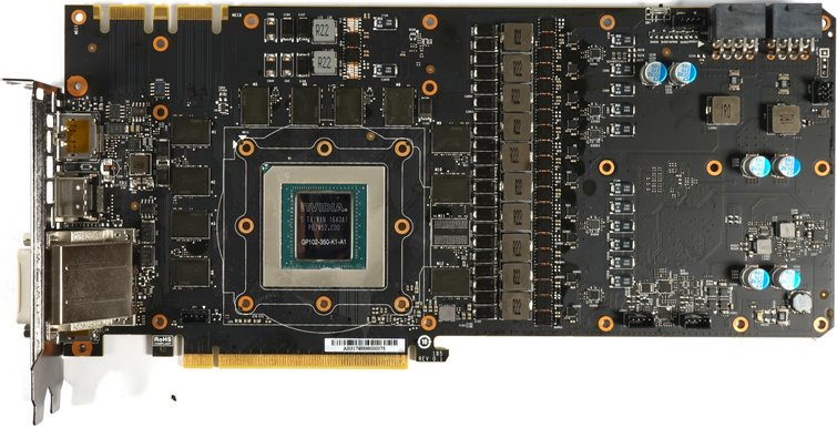
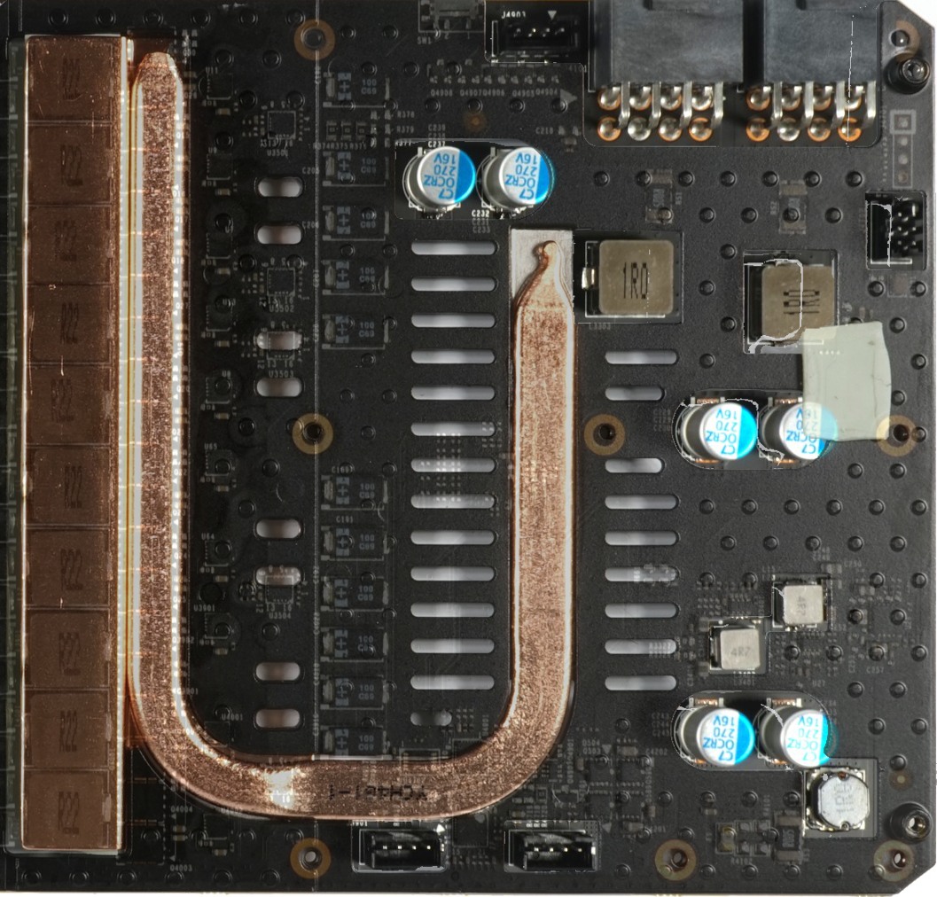
Why this is so, and we just take a look at it, is due to the heatpipe solution used, including the flange-mounted copper heat sink, which has been placed on the cooling plate. We will come back to this later, but we can already see that the coils, as we had already proposed in our measurements for the EVGA GTX 1080 FTW2 iCX, are now actively incorporated into the cooling concept.
The area for heat absorption is much larger and the coils themselves also produce a lot of waste heat. This time we have to put in this little excursion to cooling, because the electrical design of the voltage converters is also primarily subject to the aspects of cooling, or to remain correct, to the active waste heat avoidance. The super projection of the board and heatpipe shows the exact positioning:
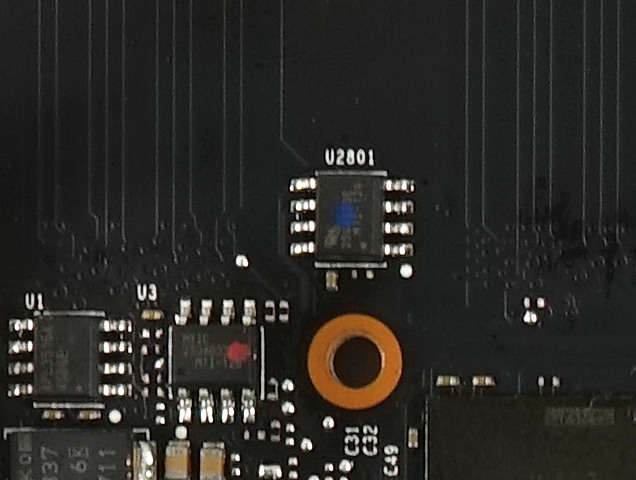
GPU Voltage Regulator
If one considers the solution to rely on a total of five flexibly regulated phases with subsequent doubling, rather superficially and remove from the data sheets of the used components their possible maximum load capacity, then one may become a hasty To conclude that this power supply is slickly crazy, overpowered and directed at the possible potency above all to ice age overclockers. However, the behind it is a certain lime(h)l, then quickly escapes.
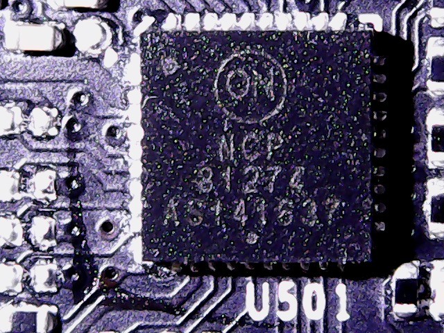
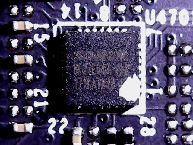
The NPC81274 from ON Semiconductur (ONSEMI) is a modern multi-phase Synchronous Buck controller that can regulate up to 8 phases simultaneously and supports three operating modes using PSI (Integrated Energy Saving Interface): (a) all phases at full load, (b) dynamic phase count/distribution at partial loads, and (c) the use of one or only a few phases for low loads (up to idle). This is important when it comes to the distribution of burdens and the sharing of hotspots, as we shall see in a while.
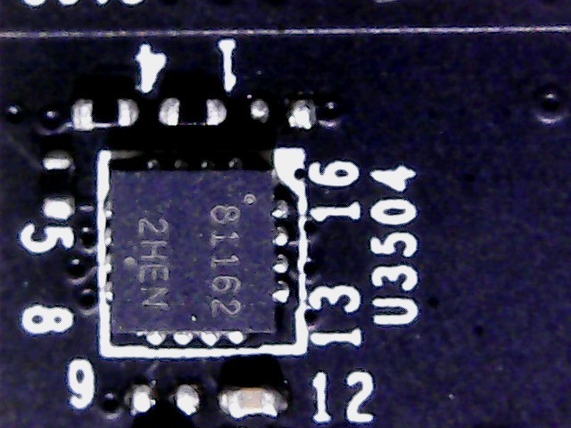
Since a total of eight phases or Control loops deemed too low, a compromise has been reached and only relies on five real phases, which are split into two control loops per phase by means of a Doppler chip (phase doubling), resulting in a total number of 10 control circuits (rails) corresponds to the This splitting can be achieved with a suitable doubler chip, in this case with an NPC81162, also from ONSEMI. The trick behind this is that you can use per phase, for example, 40 ampere can be switched, but this current can be divided into 2x 20A, which of course significantly relieves the respective control circuits.
 |
 |
What is not technically possible, however, would be an asynchronous use of both control circuits with e.g. 10A and 30A. Apart from the fact that from a circuit-technical point of view, this would not be possible with the components used or only with tricks – one would really have to use 10 real, controllable phases for such an action, but there is a lack of the suitable PWM controllers. In addition, it would hardly make any sense from a technical point of view, because from five phases it can already be worked quite efficiently, especially since one can also use the partial load mode.
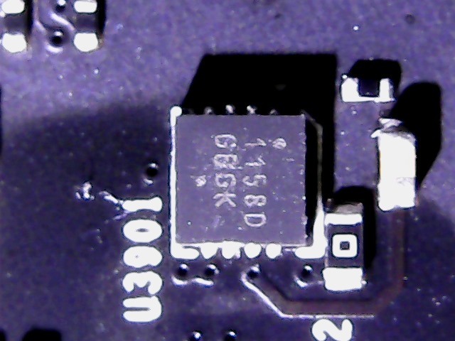
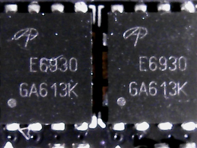
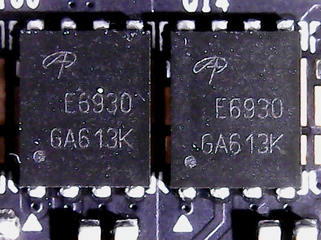
For the control of both circuits per phase, one relies on an NPC1158, which controls the two parallel Running AOE6930 from Alpha & Omega Semiconductor per control circuit. These chips are Dual Asymmetric N-Channel AlphaMOS, which combine the two MOSFETS of the high and low sides in one package. However, the fact that one bets on two such chips per control circuit (i.e. a total of 20) has nothing to do with an extremely generous overclocking offer for the number one folk sport, but has tangible technical reasons.
 |
 |
Let's pick up the 40 amperes per phase again. EVGA thus manages to halve the load to 20 amperes in a ratio of 50:50 per control circuit. Due to the use of two dual MOSFETS working in parallel, there are only 10 amperes per package at the end. This spatially equalizes the thermal hotspots, reduces the internal resistance of the parallel circuits and thus, of course, the resulting power dissipation in the form of waste heat. With so many control circuits, one can also rely on a slightly lower switching frequency of the DC/DC converters, which would create up to 1.2 MHz in theory, but would then also collapse thermally. Here it is certainly below 400 KHz, which brings additional relaxation on the radiator front.
The AOE 6930 used are also available at chip temperatures from 75 to 80°C and up to approx. 20 Ampere current flow can still be used relatively efficiently, but everything about it is already becoming thermally questionable. However, even this amount (in all-on mode, that would be a total of 400 amperes) is more than sufficient to cover all use cases. Those who cool with LN2 are not subject to these restrictions anyway. The real reason for the whole effort is therefore the highest possible efficiency of the control circuits. Without wanting to spoil it now: the bill has worked out pretty well.
Thermal sensors and evaluation
With an 8-bit Flash-Type Micro controller from Sonix, EVGA relies on a fairly successful solution to capture sensor values in near real time. A total of nine small thermal sensors are placed above and below the board at the possible focal points.
 |
 |
However, with the changeover of the control circuits to the AOE 6930 in the VRM range, one has to choose different positions, so that in some cases the displayed temperatures do not exactly correspond to what can be measured directly under the components. But this is good to be tolerated with the actual temperatures, because it almost fits perfectly.
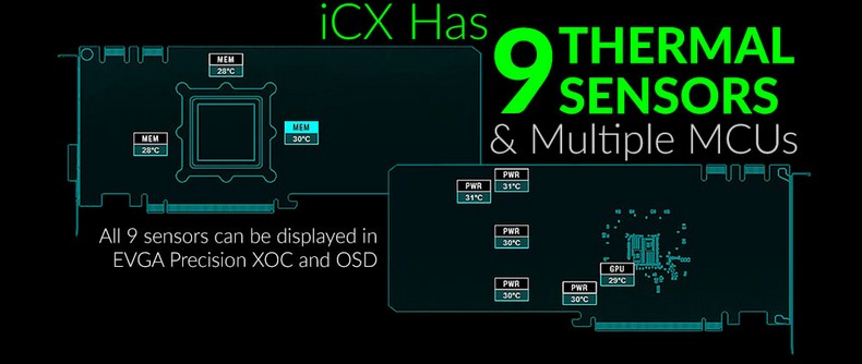
EVGA's Precision tool is able to display these nine sensor values and log them on request. In addition, fan control can be used in a targeted manner when it comes to eliminating local hotspots. If you want to know more, refer you to the test of the EVGA GeForce GTX 1080 FTW2.
Power supply of the memory
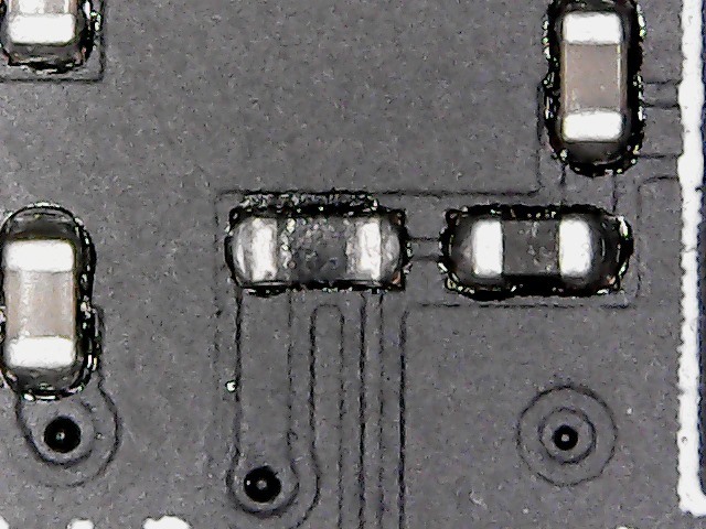
The coils rely on semi-high ferrite core coils, which are only mediocre, but fulfil their purpose quite well and are also gladly taken by the competitors (and Nvidia itself at the contract manufacturer PNY). These coils are used in both the GPU's VR and memory.
 |
 |
A total of 11 of the G5X-Micron modules of type MT58K256M321-Ja110, which offer up to 11 GByte/s and are therefore intended to compensate the missing 32 bits of the memory interface with a higher clock speed of 5500 MHz (effectively), are installed on this card. We are somewhat surprised that Nvidia does not immediately install the MT58K256M321-Ja120, which clocks a little higher. After all, the board partners buy the GPU and the memory in the bundle from Nvidia, which leaves little room for manoeuvre.
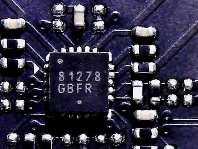
The power supply of the memory is located in the upper left corner of the GPU VR and is released via an NPC 81278 from ONSEMI, which can provide a total of two phases as a buck controller. For each of the two phases, one again relies on an AOE6930, which combines high-side and low-side. It is interesting that identical coils are used here for THE GPU-VR.
 |
 |
Other board solutions
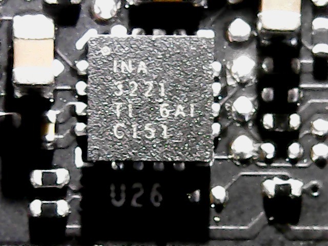
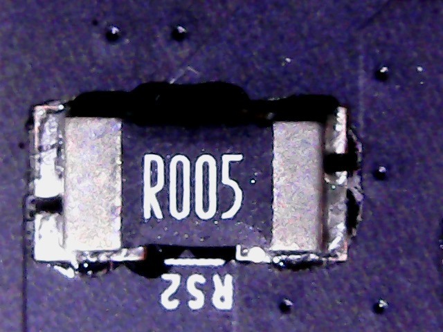
The usual INA3221 is a monitoring chip for the flowing currents, as well as the adjacent voltages and in the end also protects the technology from overloads. The two shunts in the entrance area are used to determine the current flow to be monitored and with the two coils behind the two 8-pin power supply sockets, EVGA relies on a kind of filtering of the spikes in the input area.
 |
 |
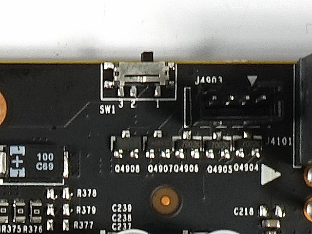
The card has a dual BIOS, which can be switched via a small slide switch (master/slave). However, if possible, the Master BIOS should not be overwritten with experimental flash attempts for violence.
 |
 |


Kommentieren