


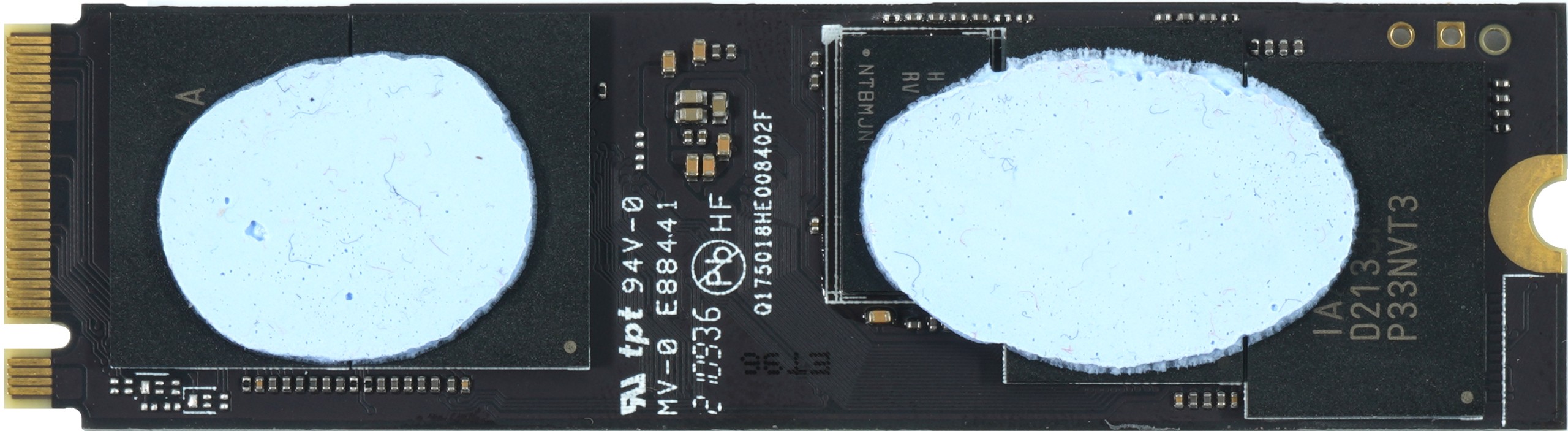
I had already written that the SSD stays a bit cooler because the NAND also acts a bit more restrained and the heat conduction connection is really good. Once you have removed the cooler, you can see the PCB, which is again from TECHVEST. You can see the memory, the controller and the DRAM modules. But first things first, let’s start with the controller.
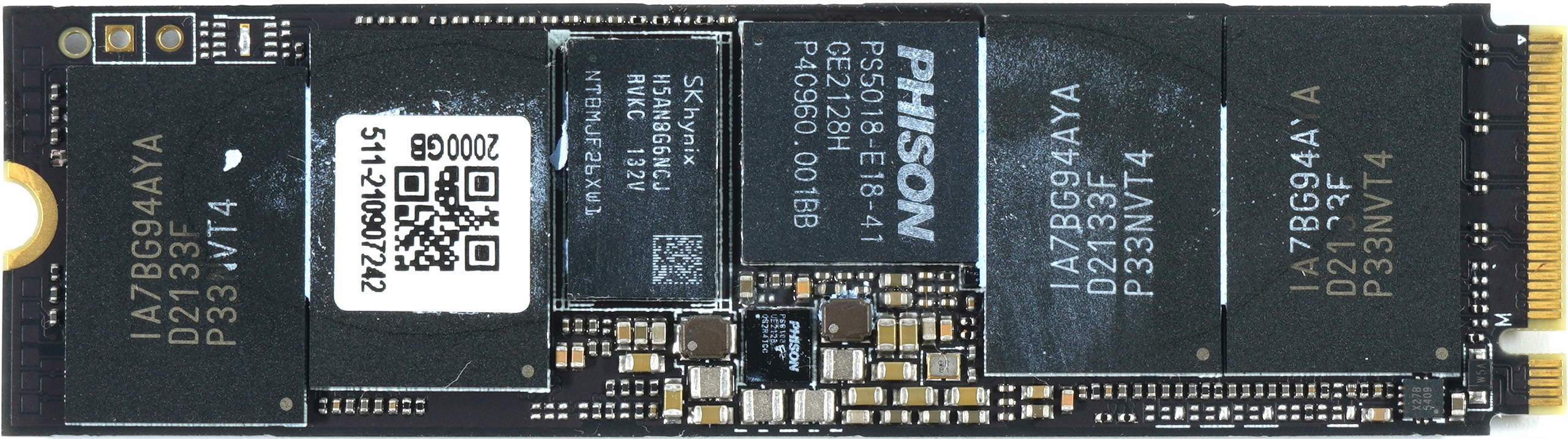
The used PS5018-E18 from Phison was developed from scratch and is manufactured in TSMC’s 12 nm node. It is, in terms of features and performance, a very interesting and fast PCIe 4.0 x4 SSD controller. To realize this, Phison has included five Arm Cortex R5 CPU cores, three of which act as the primary cores for the main tasks, while the other two are clocked lower for the Dual CoXProcessor 2.0 code to act as a more economical tandem to take at least some of the load off the three main cores.
The controller communicates with the NAND via eight NAND flash channels at up to 1,600 MTps and supports capacities of up to 8 TB with 32 chip enable. Our sample contains eight cases, four on each side, thanks to the small size of the controller, which measures only 12 x 12 mm. The design also uses a DRAM-based architecture, with the Spatium M480 Play once again featuring two DDR4 chips from SK hynix, one on each side of the PCB. These are 8 GB modules in the form of the H5AN8G6NCJR, i.e. CMOS Double Data Rate IV (DDR4) Synchronous DRAM.
Phison’s PS5018-E18 complies with the NVMe 1.4 specification and has a number of common features. Thus, it supports both Trim and S.M.A.R.T.. Like other controllers, it uses Active State Power Management (ASPM), Autonomous Power State Transition (APST), and the L1.2 ultra-low power state (see data sheet page 1). Thermal throttling is implemented, but is of no further concern since the controller does not get too hot in most applications. This can also be seen in the fact that, unlike the older models like the E16, you can do without an integrated nickel heat sink.
It also leverages the fourth-generation LDPC ECC engine, SmartECC (RAID ECC), and end-to-end data path protection for robust error correction and improved data reliability. It even supports hardware-accelerated AES 128/256-bit encryption (which is TCG, Opal 2.0, and Pyrite compliant) and has a built-in crypto-erase feature.
Like the E12S and E16 models, Phison’s E18 supports fully dynamic write caching. The size of the dynamic pSLC cache, which I will also discuss in a moment, is therefore 1/3 of the available capacity of the TLC drive. Phison has also implemented SmartFlush, which enables fast cache recovery for predictable and consistent performance. So much for the theory. Well, not quite.

Micron’s 176-layer TLC 3D NAND (codename B47R)
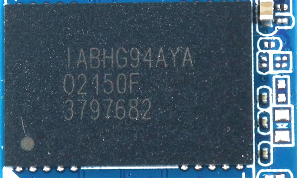
The Phison PS5019-E19T just described is compatible with a wide range of flash memory variants and supports modern NAND chips with 1200 MHz interface. And because it’s so nicely compatible, if you’re a low-cost NVMe SSD vendor, you can also use Micron’s latest 176-layer TLC 3D NAND (codenamed B47R) with it. For example, the MSI Spatium M450 I tested contains two IABHG94AYA chips, each with eight 512-gigabit TLC 3D NAND blocks inside.
By the way, Micron’s still quite new 176-layer flash is the first real in-house development by Micron after the separation from Intel. This memory is also very different in its internal structure from the products of all other manufacturers. The cell structure of the Micron NAND relies on replacement gate, which ends up being a cross between floating gate and charge trap technologies. Micron replaced the polysilicon in the gate material with metal in this NAND and switched to a different process for etching the vertical cylindrical channel, resulting in an increased diameter.
In addition, a non-conductive layer of silicon nitride has been introduced into the structure of the micron memory, in which data can be stored. This layer also reduces quite effectively the mutual interference of the cells in such a vertical stack. Of course, we can go into a little more detail. The next figure shows a chip looking at the metal top, a chip looking at the CMOS circuits (CuA) and the markings of the B47R chip. Compared to the older B37R TLC die, the chip size has been reduced by a whopping 25% due to the higher cell density, larger number of 3D NAND cells and effective scaling of the design. The B47R is now Micron’s second generation CTF structure after the B37R.
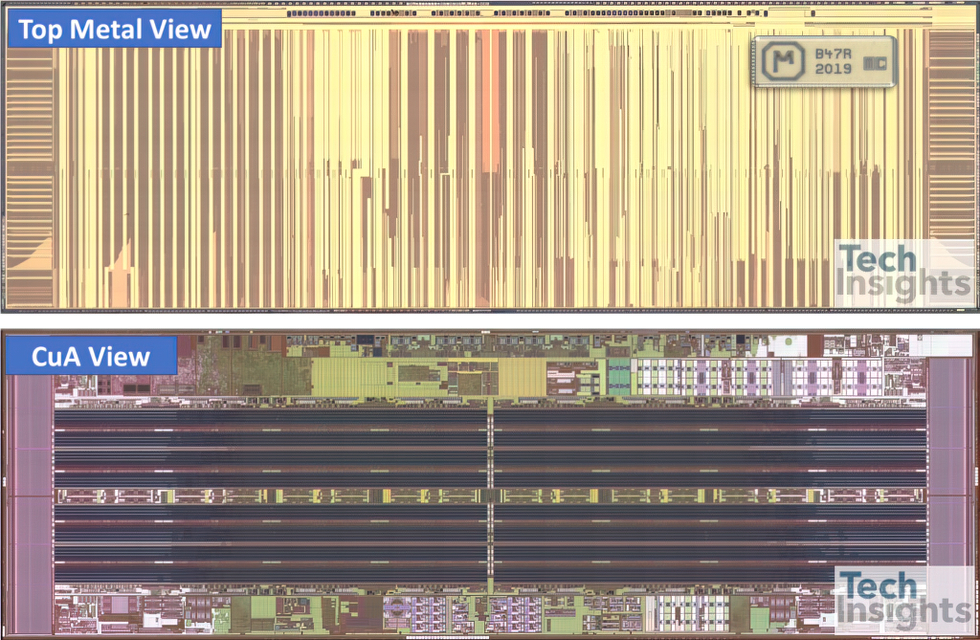
The height of the NAND cell array (for comparison: the height from the selector on the source side to the BL) is now more than 11 µm. The total number of gates, including selectors (STs) and dummy word lines (DWLs) per vertical NAND strand is 195, or 195T, which is the highest number ever achieved in 3D NAND. They rely on double-stack architecture, the replacement gate process, charger trap nitride (CTN) and CMOS-under-array (CuA) techniques. The bit density reaches 10.273 Gb/mm2 for the 512Gb TLC die.
Thus, in the end, it was possible to achieve a number of positive effects, because it was possible to increase the speed of the programming cells, increase their stability, reduce power consumption and at the same time also improve the reliability of data storage. Ultimately, Micron’s 176-layer TLC-3D NAND thus takes the next step in 3D flash technology in general. And in terms of performance, Micron claims that the new memory has reduced read and write latency by about 35% compared to the previous generation 96-layer memory. Well…


24 Antworten
Kommentar
Lade neue Kommentare
Urgestein
Urgestein
Urgestein
Moderator
Urgestein
Urgestein
Mitglied
Urgestein
Urgestein
Mitglied
Urgestein
Mitglied
Mitglied
Mitglied
Urgestein
Mitglied
Urgestein
Urgestein
Mitglied
Alle Kommentare lesen unter igor´sLAB Community →