


The new memory controller with DDR5 support is known to be one of the biggest changes in the 12th generation Intel Core CPUs. But DDR4 is also still supported – assuming an appropriate motherboard – and there have been some changes under the hood here as well. Perfect conditions to let Comet Lake, Rocket Lake and Alder Lake compete with completely identically configured DDR4 RAM in a colorful mix of gaming, benchmarking and compute!
To make the competition as fair as possible, we disabled 2 cores on the 10-core Comet Lake CPU and disabled all efficiency cores on the new Alder Lake CPU. The latter is not even a disadvantage in most benchmarks, also because the cache can be clocked higher and thus to the same level as with the older CPUs. 5.1 GHz on the cores and 4.6 GHz on the cache or ring or uncore were applied to all CPUs. For comparison, with active E-cores you have to accept about 500 MHz of loss in cache clock to avoid instabilities. Furthermore, the memory requests of the differently fast cores often stumble over each other in demanding benchmarks, which can even have negative consequences for the result, but more about that in a moment.
DDR4 is not equal to DDR4
For the RAM, I chose a configuration that supports all CPUs while providing the highest possible performance to provide the cores with as much working data as possible. For lowest possible access latencies and to keep the comparison with Comet Lake CPUs as fair as possible, I also decided to use Gear 1, i.e. the direct transmission from memory controller to RAM clock. Since Rocket Lake hits a limit here with most i9 CPUs at 3866 Mbps, this clock speed is not available in the BIOS of our only available DDR4 Z690 board, we ended up settling on 3733 Mbps. Relatively tight tCL 14, tRCDRP 14, tRAS 28 at Command Rate 2T and 1.5 Vdimm are used as timings.
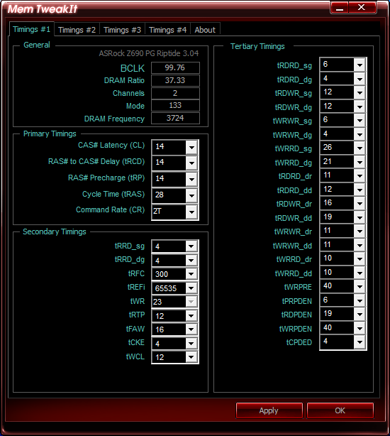
But we also set all secondary and tertiary timings to the lowest values supported by all platforms to really leave nothing to chance and make the comparison as representative as possible. Some timings like tRP or tWR could not yet be adjusted with the current BIOS of our Z690 motherboard, which is why we have adopted the resulting relatively loose value of 23 and 12 respectively for the other platforms. The “Round Trip Latency” optimization was also left constantly deactivated across all platforms to ensure as even a playing field as possible during the latency tests. Differences in the finally trained RTL values should thus be directly dependent on the actual memory latency of the respective platform.

But the DDR4 memory controllers of the platforms also differ, not only in terms of the gearing introduced with Rocket Lake. So from Rocket Lake to Alder Lake, something has changed as well. MSI had already highlighted and explained this extensively in their livestreams around the launch of the new 12th generation CPUs. Simply summarized, there are now two memory controllers instead of one, and thus one dedicated per DDR4 channel. The burst length still remains at 8 due to DDR4, while DDR5 already supports 16, but a better efficiency of the RAM should be achieved by the dedicated supply of the channels with an own controller each. Whether this is also confirmed in reality will be seen in a moment.
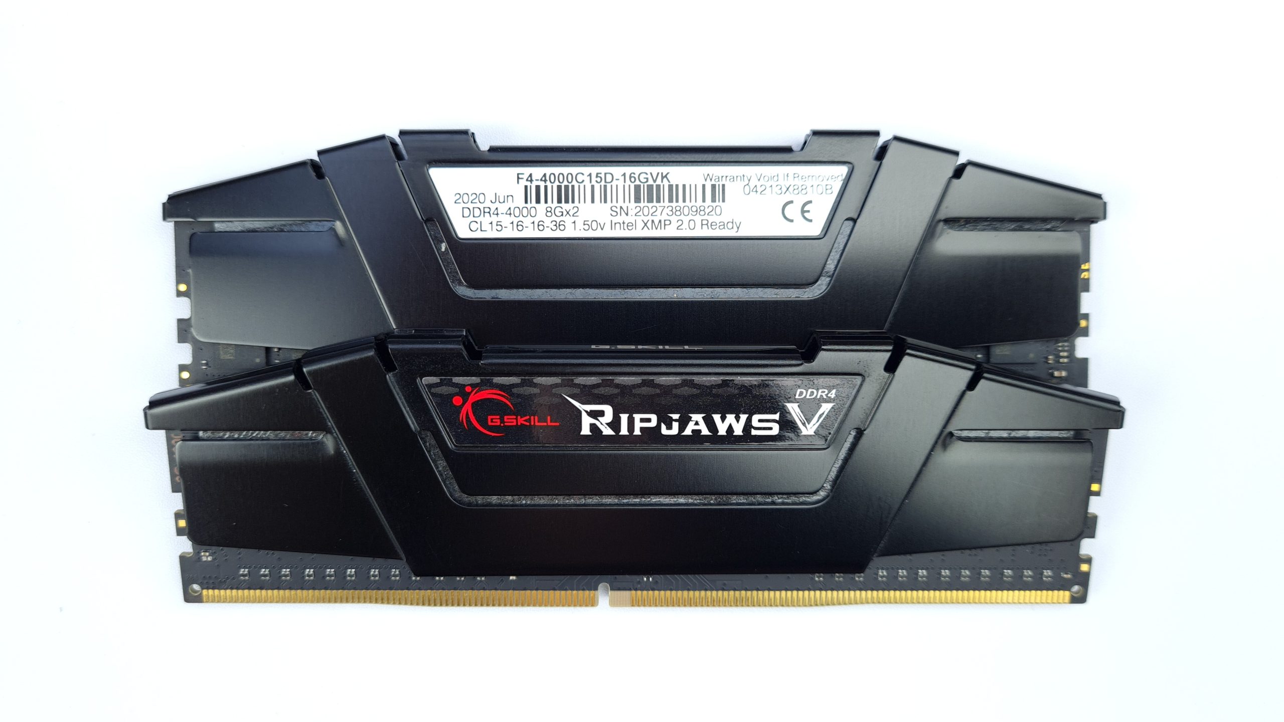
Speaking of RAM, many will have already known from the clock speeds and timings, a kit with Samsung 8 Gbit B-Die memory ICs is used. Our well-known G.Skill Ripjaws V modules with 8 GB capacity each, single-rank topology and an XMP profile of DDR4-4000 15-16-16-36 at 1.5 V are the means of choice. The set overclocking already explained above is, by the way, completely stable and could survive various RAM stress tests on each of our platforms without errors. Variances in the results due to instability are thus also prevented in advance.
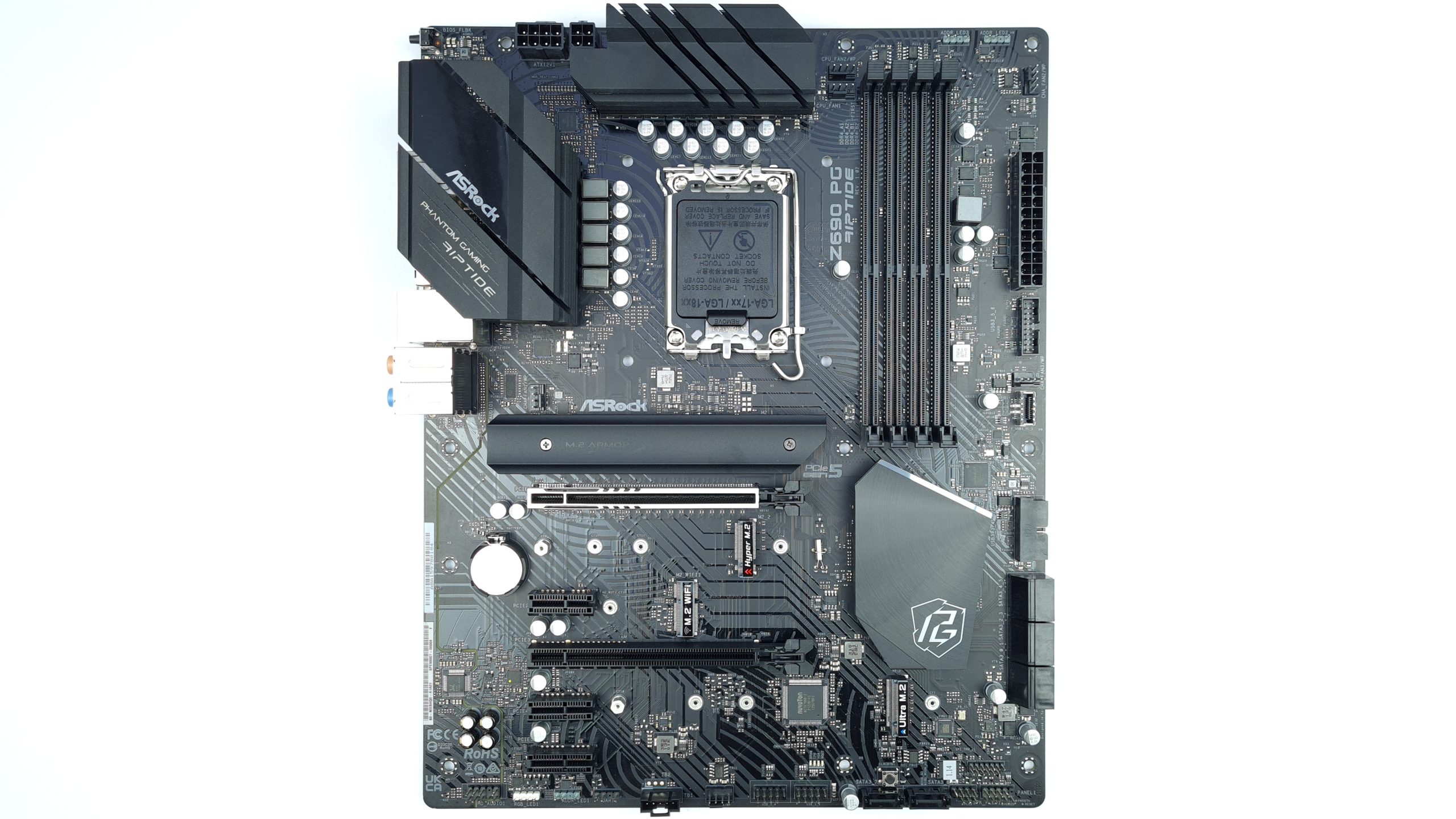
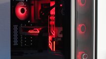
The already mentioned underpinnings for the Alder Lake platform with DDR4 is the Z690 PG Riptide, which was kindly provided to us by ASRock. As usual, a “custom” water cooling is used to prevent thermal throttling even at 1.3 Vcore VCC sense voltage. An Nvidia RTX 3090 Founders Edition with the latest driver and with maximum temperature and performance limits in MSI Afterburner serves as the pixel accelerator for the gaming tests in order to widen the GPU’s bottleneck as much as possible. As always, a complete listing of the test systems used follows in tabular form:
| Test systems | |
|---|---|
| Hardware: |
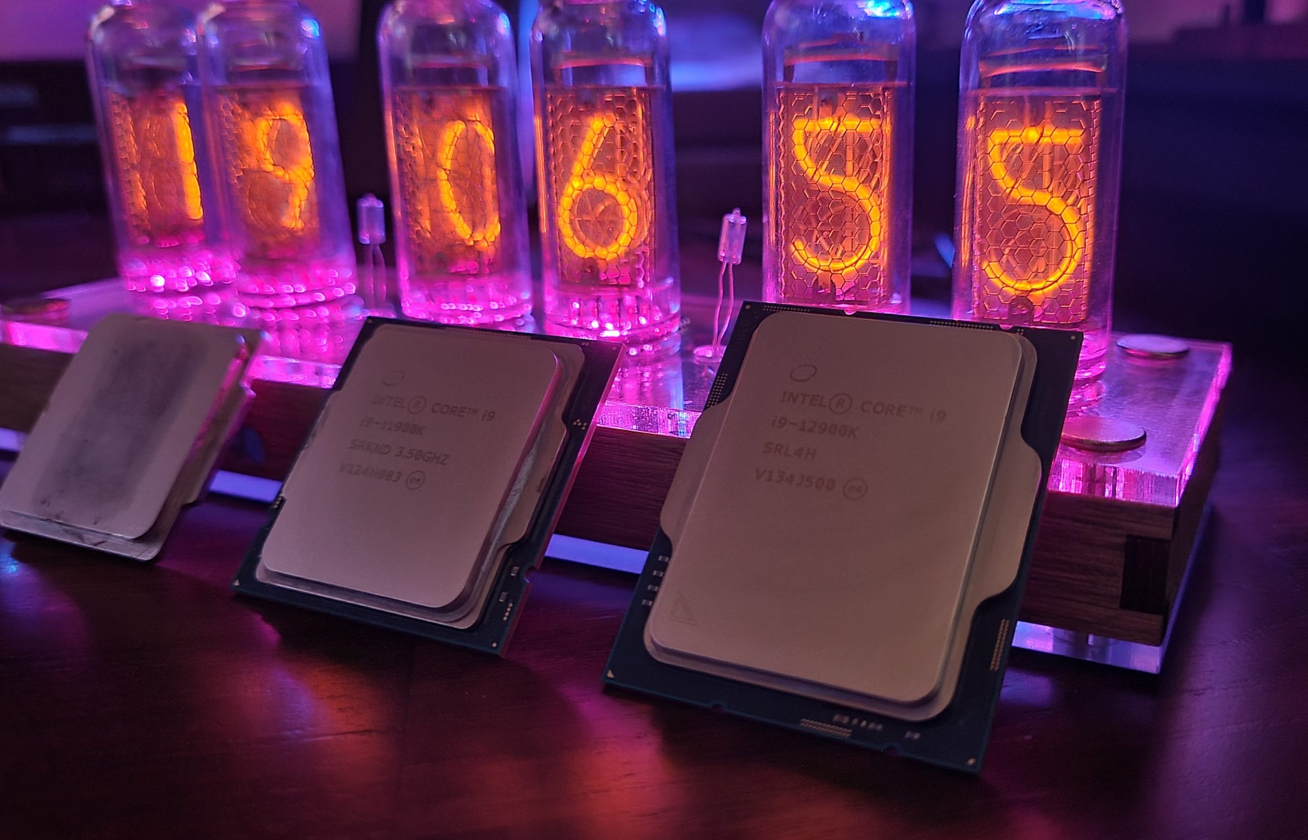
Comet Lake
Rocket Lake
Alder Lake
|
| Cooling: |
|
| Housing: |
|
| Periphery: |
|
| Measuring devices |
|
For better clarity, the following abbreviations are used in the diagrams:
- SR: single-ranked memory topology
- 3733c14*: DDR4-3733 RAM clock with all timings as described above (see screenshot)
- G1: Gear 1, 1:1 translation from memory controller to RAM
- 10900K: Intel Core i9-10900KF CPU, Comet Lake family
- 11900K: Intel Core i9-11900K CPU, Rocket Lake family
- 12900K: Intel Core i9-12900K CPU, Alder Lake family
- 8P: 8 active or performance cores
- 51/46: 5.1 GHz core clock and 4.6 GHz cache clock


22 Antworten
Kommentar
Lade neue Kommentare
Neuling
Urgestein
Veteran
Veteran
Urgestein
Urgestein
Veteran
Urgestein
Veteran
Mitglied
Mitglied
Urgestein
Mitglied
Urgestein
Mitglied
Urgestein
1
Veteran
Urgestein
Alle Kommentare lesen unter igor´sLAB Community →