


SPD information and test system
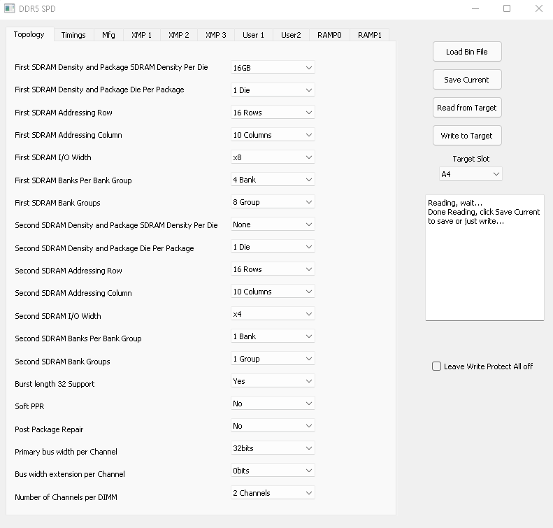
Of course, a look into the SPD of the modules should not be missing, even if we have a bit less to discover here than usual due to the missing XMP profile. For this we again use the “Tool.exe” software with the “DDR5 PMIC” function on the Asus Maximus Z690 Apex. In the topology tab we find the confirmation that x8 ICs are indeed installed, each with 8 bank groups, with 4 banks each. Four of the ICs are then combined into a 32 bit subchannel, which results in the 64 bit total interface that is usual for DDR5.
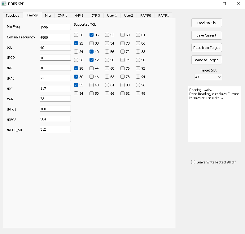
In the Timings tab we find details about the pre-configured JEDEC profile of the modules. Unfortunately, the units are still mixed up in the tool here, so that the minimum frequency refers to the actual frequency of 2000 MHz and thus DDR5-4000. However, the modules are then nominally specified for DDR5-4800 with tCL 40, tRCD 40, tRP 40, tRAS 77, tRC 117, tWR 72, tRFC1 708, tRFC 384 and tRFC3_SB 312. No relevance can be determined for the supported tCL values specified here during actual operation. Although the operating voltage is not specified here, we can infer 1.1 V for each VDD and VDDQ based on the JEDEC standard.
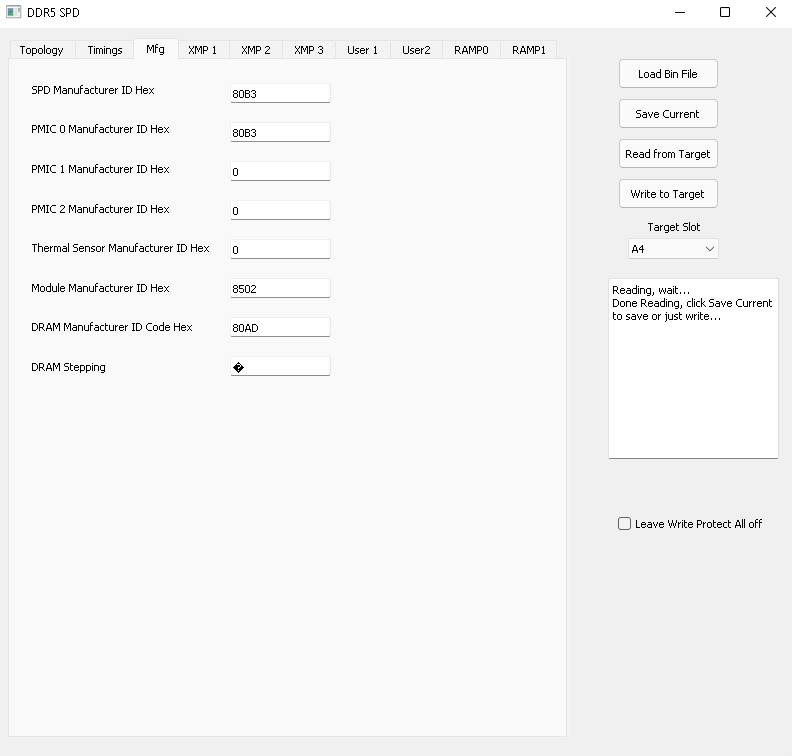
In the Mfg tab we then find known Hex IDs of the hardware components that we could already view on the board. The manufacturer ID 80B3 of SPD and PMIC is an old known one and stands for Renesas. The module manufacturer has ID 8502 on file, which is interestingly different from the Teamgroup VULCAN modules, although both are manufactured by Brain Power. However, the DRAM manufacturer with ID 80AD again matches our previous reviews and stands for SK Hynix. In the case of DRAM stepping, the software cannot read the revision correctly, but we already know from the inscription on the memory chips that it is “M” for Hynix DDR5 16 Gbit M-Die.
An Asus Maximus Z690 Apex and an Intel Core i9-12900K are used as the test system, whereby both are selected for the highest possible RAM clock in order to not represent a bottleneck for the tested RAM kits. The full list of hardware used follows as always:
|
Test systems |
|
|---|---|
| Hardware: |
|
| Cooling: |
|
| Housing: |
|
| Periphery: |
|
| Measuring devices: |
|
For better clarity, the following abbreviations are used in the diagrams:
- 12900K: Intel Core i9-12900K CPU
- 51/0/49: Multipliers for P-cores x51, E-cores 0 (deactivated), cache x49 at BCLK 100 MHz
- XPGL: XPG LANCER RGB DDR5 modules from ADATA
- DPR: Dominator Platinum RGB DDR5 modules from Corsair
- FB: Fury Beast DDR5 modules from Kingston
- DR: Dual-Rank, if not specified Single-Rank
- 3600c14: configuration with 3600 Mbps and tCL timing 14, see screenshots for all timings
- 1T, 2T: Command rate 1T or 2T
- *: completely manually set subtimings, see screenshots
- G1, G2: Gear 1, Gear2 – ratio between IMC clock and RAM clock, Gear 1 = 1:1, Gear 2 = 1:2
- H16M: SK Hynix 16 Gbit M-Die memory chips
- S16B: Samsung 16 Gbit B-Die Memory Chips
Timings of the DDR4 comparison config:


5 Antworten
Kommentar
Lade neue Kommentare
Urgestein
Urgestein
Neuling
Veteran
Mitglied
Alle Kommentare lesen unter igor´sLAB Community →