Teardown: PCB layout and components
Now let’s get straight to the PCB analysis. And right here I have to and want to give you (as always) a few details on the way, which are fundamentally different with AMD than with NVIDIA. Anyone can count phases (or at least thinks they can), but this is a little misleading. AMD uses three expensive dual-rail PWM controllers to generate the five (!) most important voltages and also real Smart Power Stages (SPS), which can report back the flowing currents (IMON) and temperatures (TMON) in real time.
Of course, telemetry is really happy about this, because AMD does not take NVIDIA’s simple route with the shunts to monitor the power limit of the entire card including all losses BEFORE the voltage converters (primary side), but instead checks all the currents individually directly AFTER the voltage conversion. Unfortunately, the rest is pure estimation. But it works much better than with NVIDIA’s RTX 4060, where there was a clear output error at the end because shunt monitoring had been omitted for the first time in a long time. Art comes from skill.
As people have repeatedly asked which voltages these are in detail, I will explain the less well-known voltages today. The acronym “VDD” stands for “Voltage Drain-Drain”, which comes from MOSFET terminology, and is used to describe the supply voltage. This term will come up again and again, so I’d better explain it in advance. And now let’s go into the details of the “magic five”.
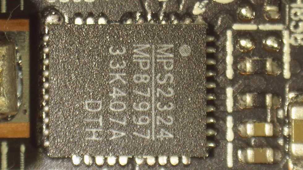
The power supply naturally relies on VDDCR_GFX (i.e. the equivalent of NVIDIA’s NVVDD) as the largest item for the GPU. Nine phases are used here, each of which controls a single PLC (voltage regulator). For this purpose, the MP2857 with 8 4 phases from Monolith is used for the required 9 phases with AMD’s SVI2 interface and the MP87997 as the PLC from the same manufacturer. It is a digital, multiphase dual-rail controller that primarily provides the power supply for the PWM VID core and is also compatible with the AVS bus interface. It can also work with Monolith’s Intelli-Phase products to implement the multiphase voltage regulator (VR) solution with a minimum of external components.
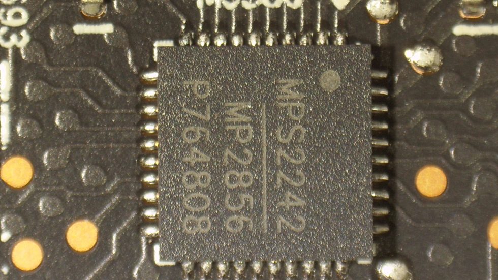
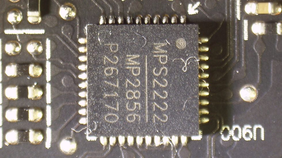
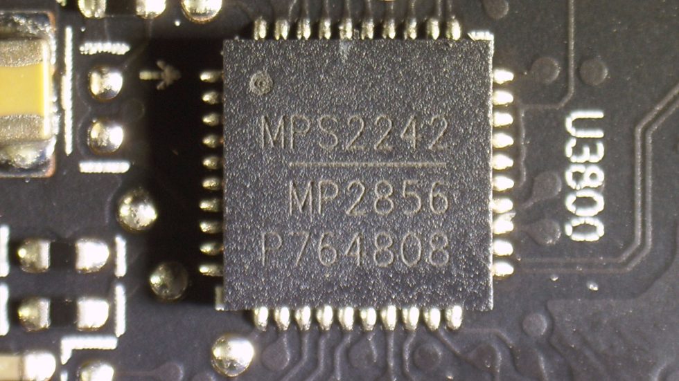
Another PWM controller (MP2856 with max. 4 4 phases) controls two separate phases for VDD_SOC and one for VDD_USR. VDD_SOC writes the supply voltage level that drives the system-on-chip. This voltage level is important to the operation of the SoC and must be precisely specified and regulated to ensure that the chip functions properly. Even more mysterious, however, is VDD_USR. The USR stands for Ultra-Short Reach and should actually be called USR_PHY. This is because it is a voltage for inter-die communication and PHY stands for the physical layer of a connection protocol. In short, the MCM components of the chiplet design also want and need to exchange data with each other.
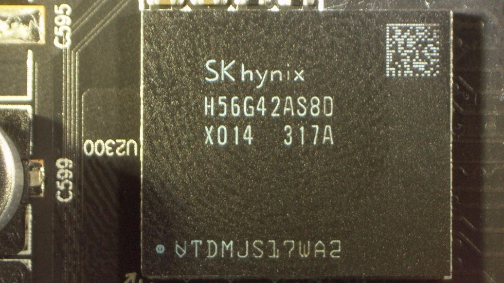
At the rear, VDD_MEM and VDDCI_MEM are located near the PWM controller for supplying power to the memory. Here (as with VDD_USR and VDD_SOC) a cheaper MP2853 from Monolith would have sufficed, but the large controller (MP2856 with max. 4 4 phases) is also fitted. A waste of money, but at least available. VDDCI_MEM is not a big item in terms of performance, but it is extremely important. It is used for the GPU-internal level transition between the GPU and the memory signal, something like the voltage between the memory and the GPU core on the I/O bus.
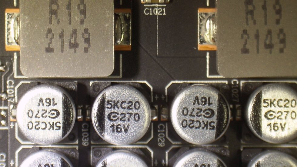
In addition, further low voltages are generated (see diagram on the front). The majority of these very similar voltage converters are located on the front of the board. There is also a 1.8V source (TTL, GPU GPIO), VDD_13 (Aux) and an ultra-low dropout chip generates the very low voltage for the PLL area (VPP). All power stages used, including those for the memory, are also products from Monolith. The MP87997 is a very high performance monolithic half bridge and the integration of drivers and MOSFETs (DrMOS) results in high efficiency due to an optimized dead time and a reduction of parasitic inductance. This small, 5 mm x 6 mm LGA component fits perfectly with the MP2856.
- 1 - Introduction and technical data
- 2 - Test system in igor'sLAB MIFCOM-PC
- 3 - Teardown: PCB and components
- 4 - Teardown: Cooler and material analysis
- 5 - Gaming-Performance in Full-HD (1920 x 1080)
- 6 - Gaming-Performance in WQHD (2560 x 1440)
- 7 - Details: power consumption and load balancing
- 8 - Transients and PSU recommendation
- 9 - Clock rates, temperatures and infrared analysis
- 10 - Noise level and fan curves
- 11 - Summary and conclusion








145 Antworten
Kommentar
Lade neue Kommentare
Veteran
Urgestein
Urgestein
Urgestein
1
Urgestein
Urgestein
1
Urgestein
Urgestein
Urgestein
Urgestein
Urgestein
Urgestein
1
Urgestein
Urgestein
Urgestein
Urgestein
Alle Kommentare lesen unter igor´sLAB Community →