


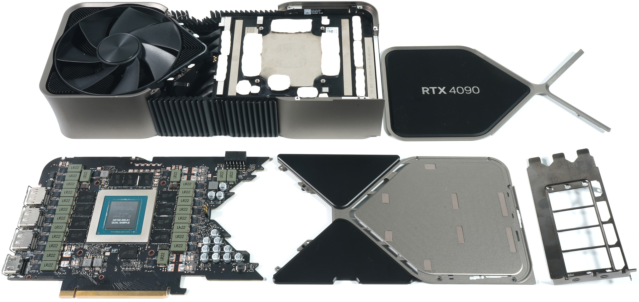
Teardown: PCB layout and components
At first glance, the board might hardly differ from the board of a GeForce RTX 3090 Ti, but it does at second glance. I will discuss the changes in load cycling and power consumption later, but let’s start with the board itself. NVVDD is still the main voltage and MSVDD has been buried for good. This also results in the voltage transformer design with a total of 10 phases and the resulting 20 control loops for NVVDD (two in parallel per phase). The GeForce RTX 3090 Ti still relied on 8 phases and a total of 24 voltage converters, so three per phase in parallel.
That one relies on a solid parallel circuit instead of phase doubling makes perfect sense, because with the now also higher switching frequencies the double number of phases would only be a hindrance due to the inertia of the coils and caps. Cheaper cards will probably rely on doubled 8-phases again, because the PWM controllers and also the DrMOS cost hard cash. But NVIDIA really let it rip at the FE.
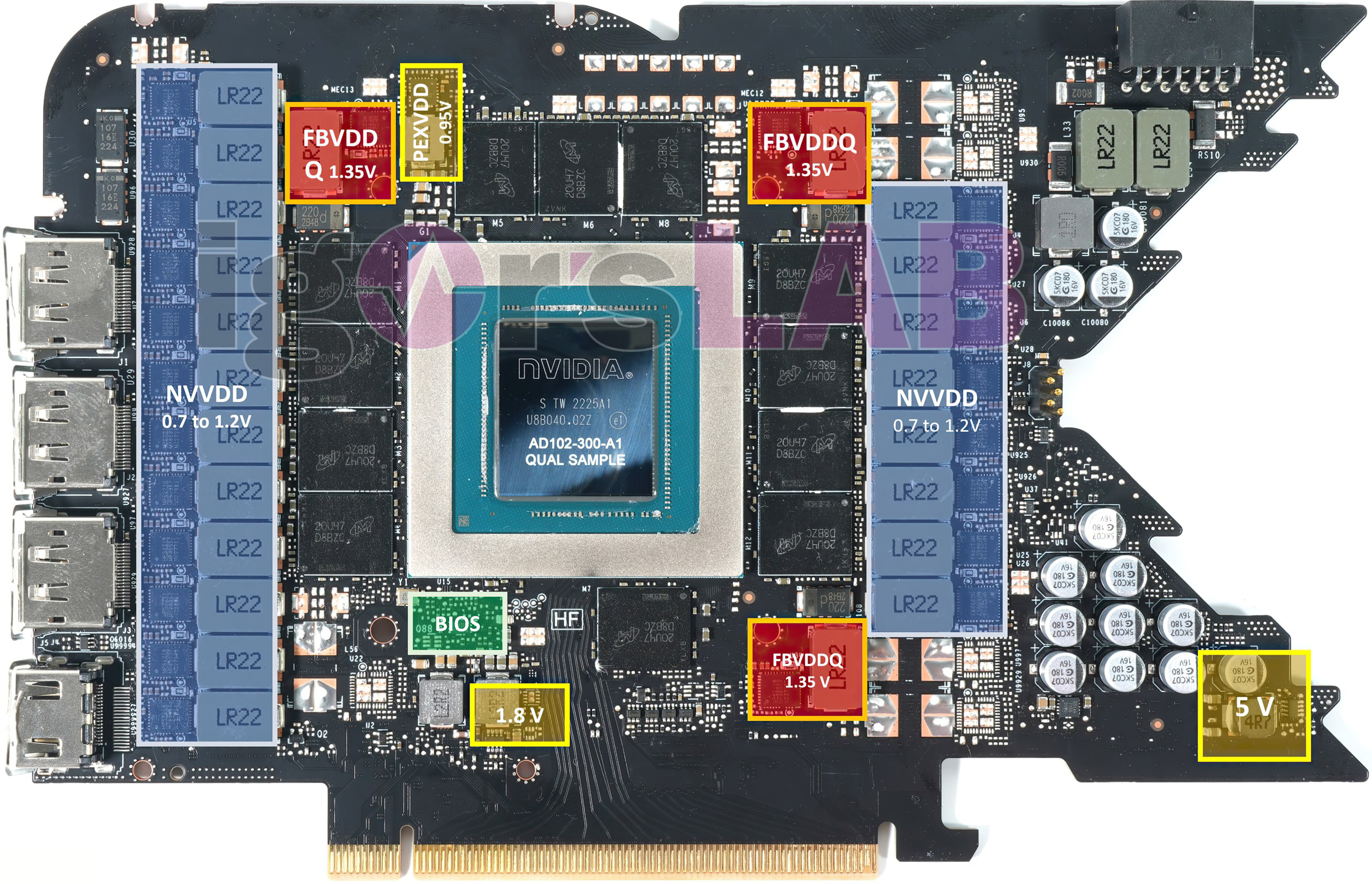
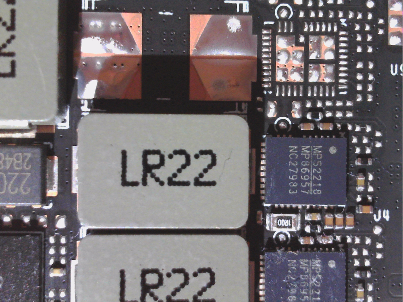
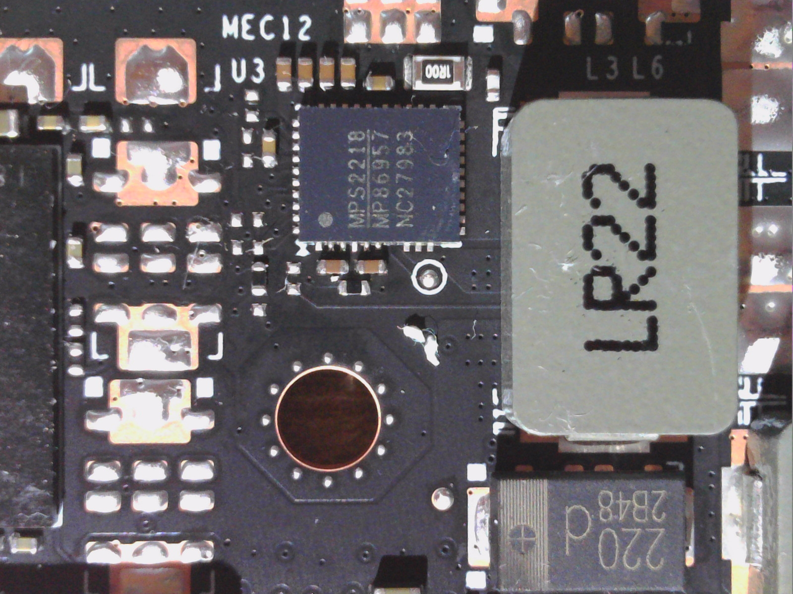
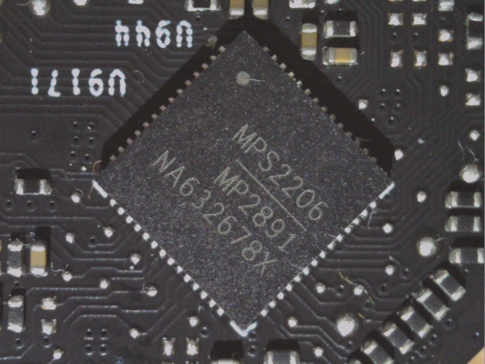
The joint PWM controller for NVVDD (GPU core) and FBVDDQ (memory) in the form of Monolith’s MP2891 is currently one of the top models among PWM controllers. It is a digital, multi-phase dual-rail controller that primarily provides power to the NVIDIA PWM VID core and is also compatible with the AVSBus interface. The MP2891 can (and should) also work with MPS’ Intelli-PhaseTM products to complete the multi-phase voltage regulator (VR) solution with a minimum of external components.
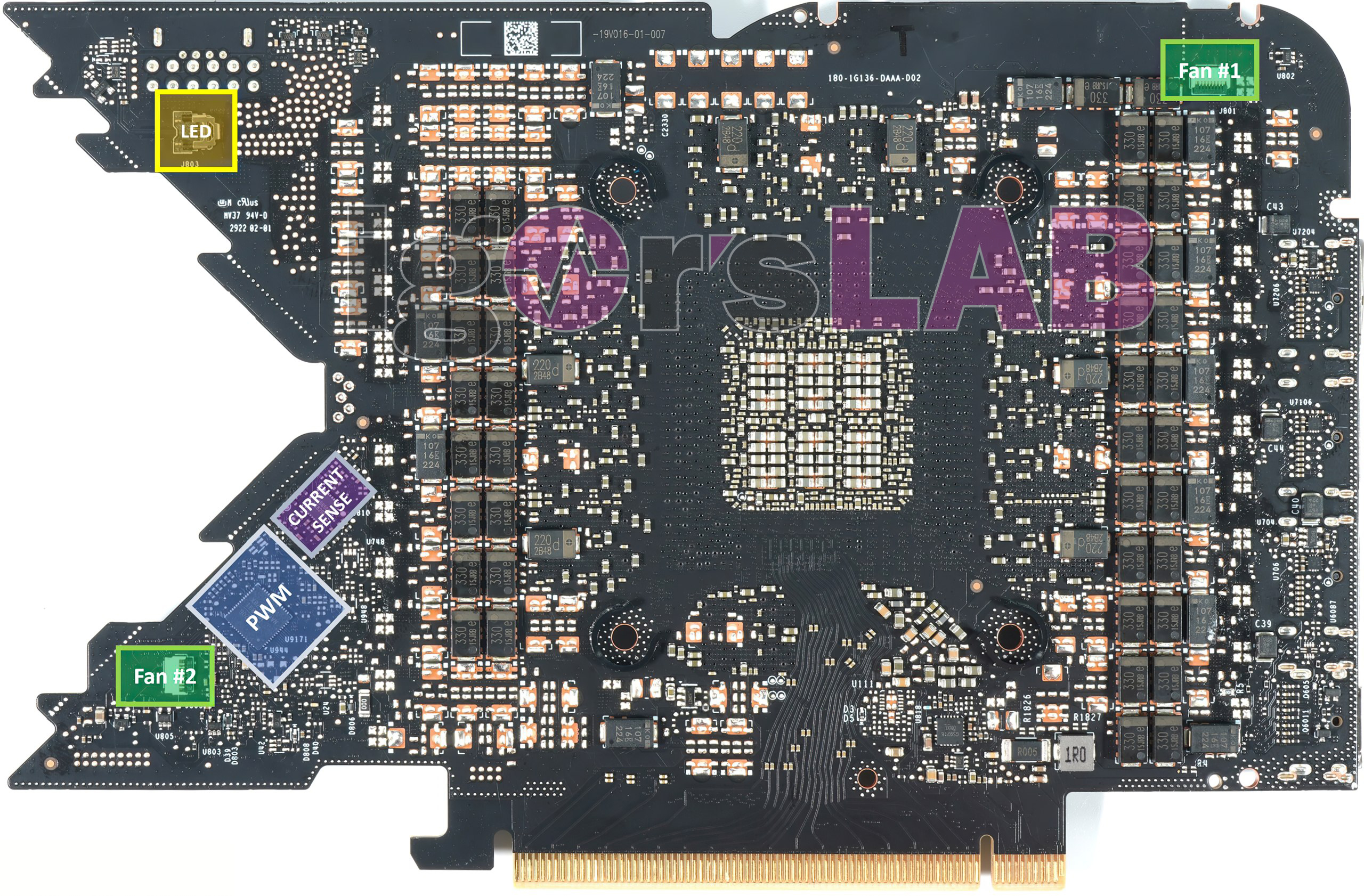
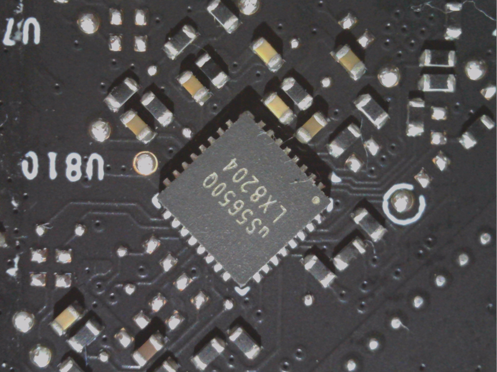
The MP2891 is even underpowered with the 10 phases on rail 1, because it could control up to 16 directly. Track 2 is then used to control the three phases for the memory (up to eight would be possible there). It is located on the back of the board. Right next to it is a uPI uS5650Q for monitoring the four 12V rails (3x Aux and 1x PEG).
All power stages used, including those for the memory, are also Monolith products. The MP86957 is a monolithic half bridge capable of driving up to 70A per phase. The integration of drivers and MOSFETs (DrMOS) results in high efficiency due to optimal dead time and reduction of parasitic inductance. This small, 5 mm x 6 mm LGA device can operate at frequencies from 100 kHz to 3 MHz, making it a perfect match for the MP2891.
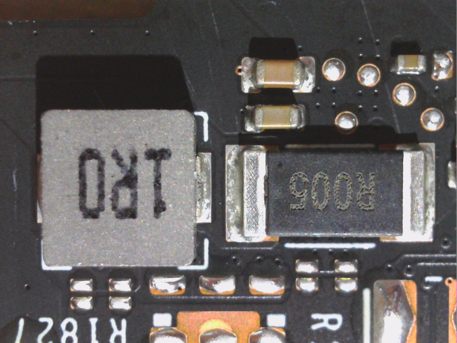
The three 12V rails on the 12+4 12VHPWR connector are combined into one rail after the three shunts (one per rail), another is connected to the PEG but is not used for NVVDD. The single BIOS is at the usual place and also the generation of the remaining extra-low voltages is as usual. So there are no more special features. The two ribbon cables of the fans are self-explanatory.

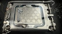
Teardown: The cooler
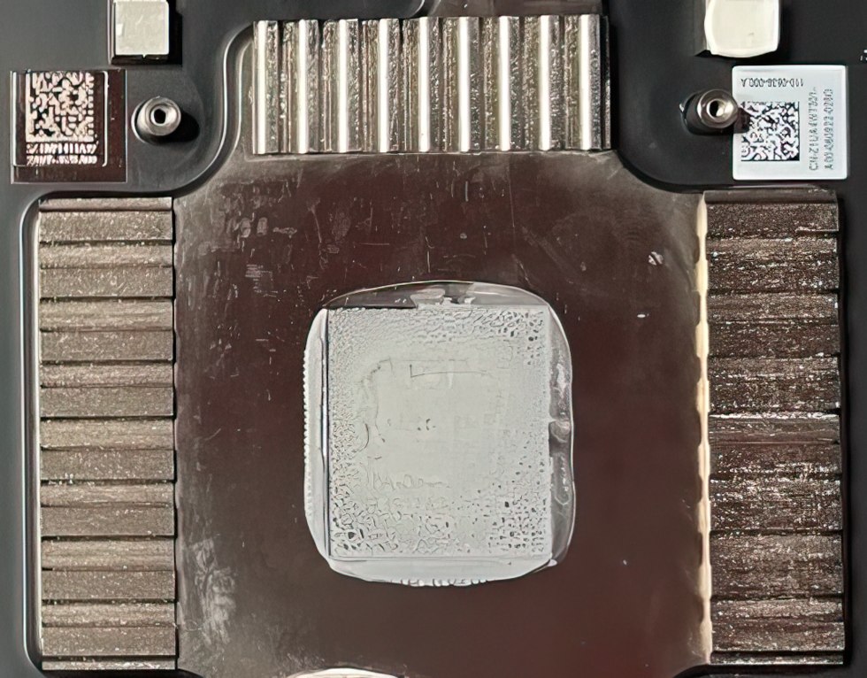
There is a big innovation here, because this time they decided to use a massive vapor chamber instead of a simple copper heat sink. That really pays off in the end, as we’ll see later with the temperatures. The memory is directly thermally connected to the bottom of the vapor chamber, which is a good choice. Furthermore, all relevant voltage transformers are cooled via the massive support frame.
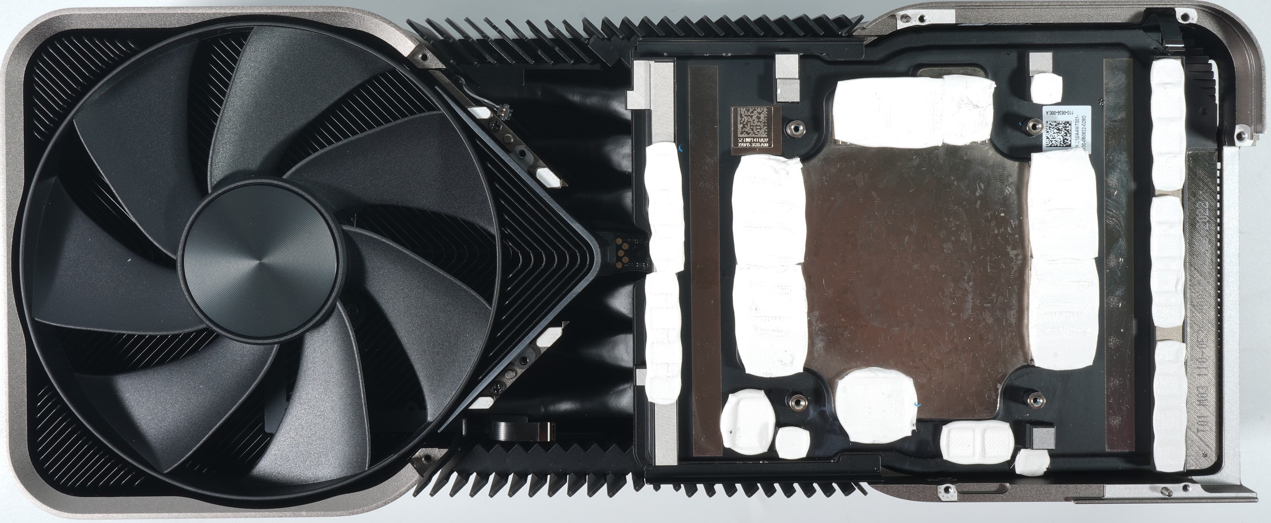
The storage again relies on Ziitek’s thick “crumble” pads for cooling, and they even go so far as to dovetail the contact surface to achieve a larger area. This has not yet been seen on graphics cards in this form. But it works, as we will see later.
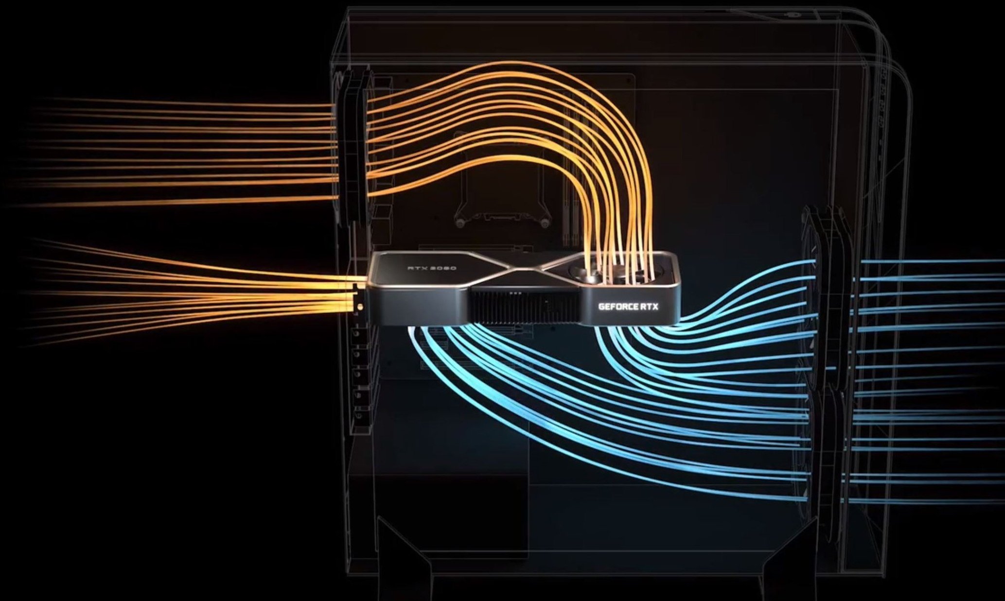
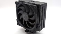
The two 11.5 cm fans each have seven steeply pitched, very large rotor blades and are still relatively tolerable up to about 1500 rpm, and even downright quiet up to about 1000 rpm. The card occupies three slots and most of the weight is at the expense of the actual cooling design. The swipe principle has been written about often enough, so I’ll spare myself the redundancy at this point.

- 1 - Introduction, technical data and technology
- 2 - Test system in igor'sLAB MIFCOM-PC
- 3 - Teardown: PCB, components and cooler
- 4 - Gaming Performance WQHD (2560 x 1440 Pixels)
- 5 - Gaming Performance UHD (3840 x 2160 Pixels)
- 6 - Gaming Performance UHD + DLSS/FSR/XeSS (3840 x 2160 Pixels)
- 7 - DLSS 3.0 and the longest bars
- 8 - NVIDIA Reflex and Latency
- 9 - Workstation graphics and rendering
- 10 - Power consumption and load sharing
- 11 - Load peaks, capping and power supply recommendation
- 12 - Temperatures, clock rate, OC, fans and noise
- 13 - Summary and Conclusion


545 Antworten
Kommentar
Lade neue Kommentare
Urgestein
Veteran
Urgestein
Urgestein
Urgestein
Urgestein
Veteran
Urgestein
Veteran
Urgestein
Mitglied
Veteran
Urgestein
Veteran
Urgestein
Urgestein
Mitglied
Mitglied
Veteran
Alle Kommentare lesen unter igor´sLAB Community →