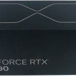
The time has come and after an almost unbearable period of waiting and speculation, I can finally present the GeForce RTX 4090 Founders Edition (FE) today including all technical details and the long-awaited benchmarks. I already wrote an article about the origin of the mega-sized coolers, but that will remain only a (albeit important) side note today until the paragraph with the temperatures. This is because our focus is so diverse that we will be publishing not just one or two articles, but several.
Important preface
Today, we will first primarily focus on the technical overview including the GeForce RTX 4090 FE as a test object. Of course, as usual including benchmarks, teardown, board and cooler analysis, as well as power consumption and load peaks with power supply recommendation. Of course, we also include the important things like DLSS 3.0 and Reflex in the benchmarks (including short introductions), but I already have to refer to the many other follow-ups that will then deal with further benchmarks, image quality comparisons to FSR and Xe, and latencies.
This subject has become so complex that you simply can’t do it justice with a quick skim. Then we even have a special video analysis for you, the basis of which I still built into the CMS at the weekend. So it’s worth enjoying the NVIDIA week until the end. And we will of course use all this effort as a basis to then compare all this again directly with AMD’s upcoming RDNA3 graphics card generation in November.
The AD 102 and the new Ada architecture
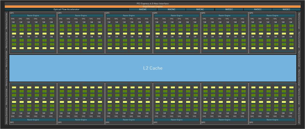
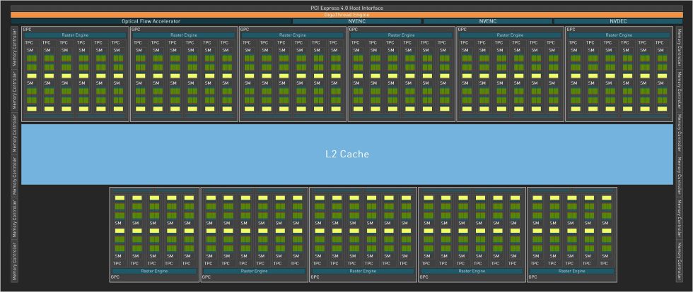
The NVIDIA GeForce RTX 4090 is manufactured in the TSMC 4N process and features 76.3 billion transistors and, I can already spoil, offers a huge leap in performance, efficiency and also AI-powered graphics. The Ada architecture relies on up to 12 Graphic Processing Clusters (GPC) and up to 144 new streaming multiprocessors (SM) with over 18,00 CUDA cores, whose performance and energy efficiency have increased significantly.
In addition, there are tensor cores of the 4. Generation and Optical Flow, enabling transformative AI technologies including NVIDIA DLSS and the new NVIDIA DLSS 3 frame rate multiplier. The RT cores of the new generation offer up to 2x ray tracing performance, Shader Execution Reordering (SER) improves ray tracing operations by a factor of two. In addition, NVIDIA now also uses a dual AV1 encoder, whereby the NVIDIA encoder (NVENC) of the 8th generation is used. Generation with AV1 is said to work up to 40% more efficiently than H.264.
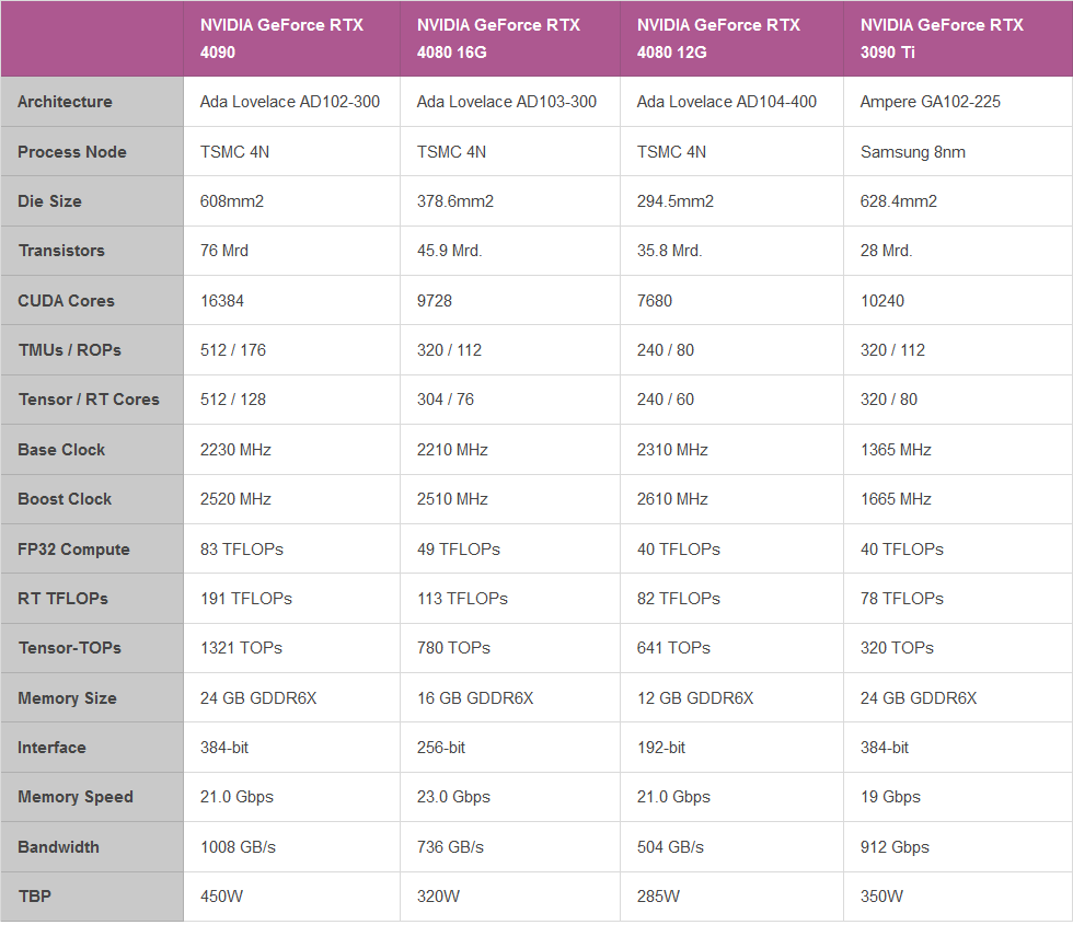
The AD102-300 of the GeForce RTX 4090 has been limited a bit and still offers 11 GPC in total, but two of them have been cut from 12 to 10 SM. This still results in 128 SM including the 16384 CUDA cores for the chip of the new consumer card. In addition, there are a total of 64 Texture Processing Clusters (TPC), 128 RT cores of the 3rd generation, 512 tensor cores of the 4th generation, 512 Texture Units (TU) and 176 ROPs. The L2 cache is 73728 KB in total and the card uses 24 GB GDDR6X with 10501 MHz clock and a 384-bit interface, which corresponds to a data rate of 21 Gbps and a bandwidth of 1008 GB/s.
The changes to all three core types can be summarized quite simply:
- Programmable Shader: Ada’s SM includes an important new technology called Shader Execution Reordering (SER) that reorders work on the fly, providing a 2x speedup for ray tracing. SER is as big an innovation as the out-of-order design for CPUs was at the time. 83 shader TFLOPS are quite a statement
- Tensor Cores of the 4. Generation: The new Tensor Core in Ada includes the NVIDIA Hopper FP8 Transformer Engine, which delivers over 1.3 petaFLOPS for AI inference workloads in the RTX 4090. Compared to FP16, FP8 halves data storage requirements and doubles AI performance. The GeForce RTX 4090 thus offers more than twice the total Tensor Core processing power of the RTX 3090 Ti.
- RT Core of the 3. Generation: A new opacity micromap engine accelerates ray tracing of alpha-checked geometries by a factor of 2. Add to this a new micro-mesh engine that handles all the geometric richness without further BVH creation and storage costs. Triangulation throughput is 191 RT-TFLOPS, compared to Ampere’s 78 RTTFLOPS.
The card still relies on a PCIe Gen. 4 interface and only for the external power connection with the 12VHPWR connector (12+4 pin) on an element of the PCIe Gen. 5 specification. The TGP is 450 watts and can also be raised up to 600 watts, depending on the board partner (which is rather pointless because the voltage limits from 500 watts anyway). The extremely oversized cooler will know how to prevent the chip’s maximum permissible 90 °C anyway.
The NVIDIA GeForce RTX 4090 FE 24 GB in detail
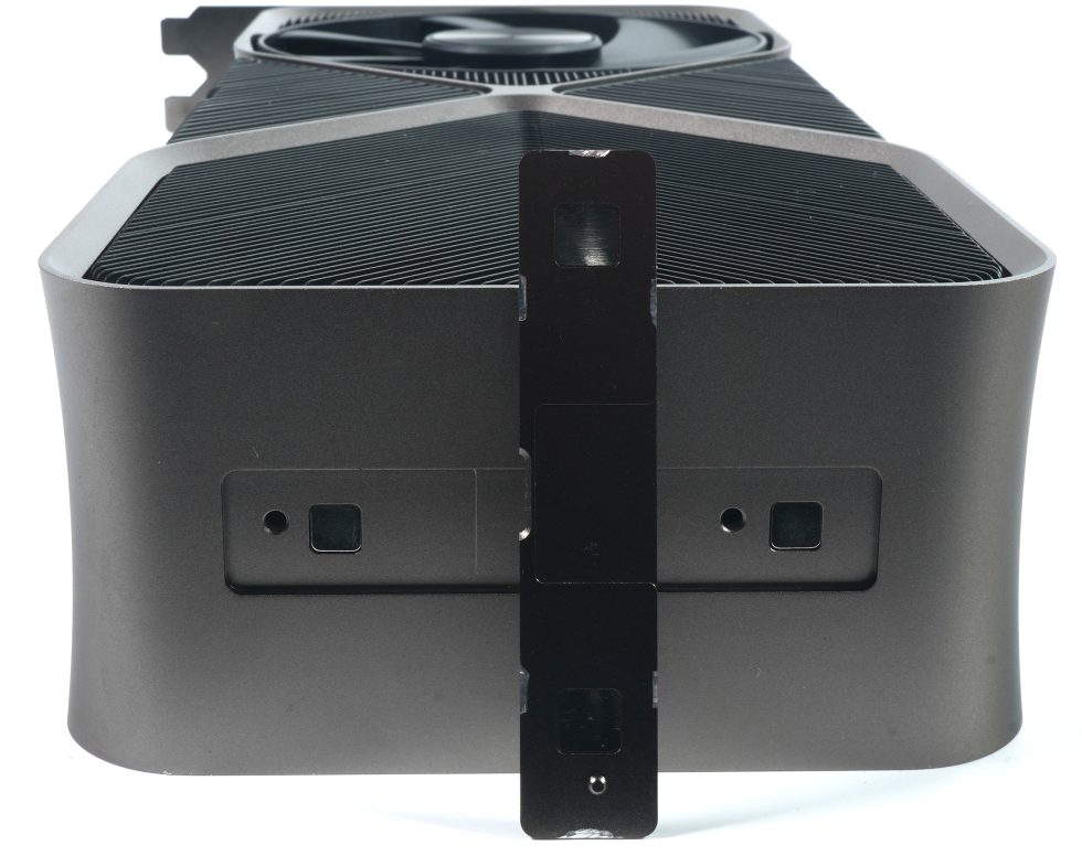
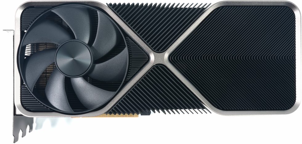
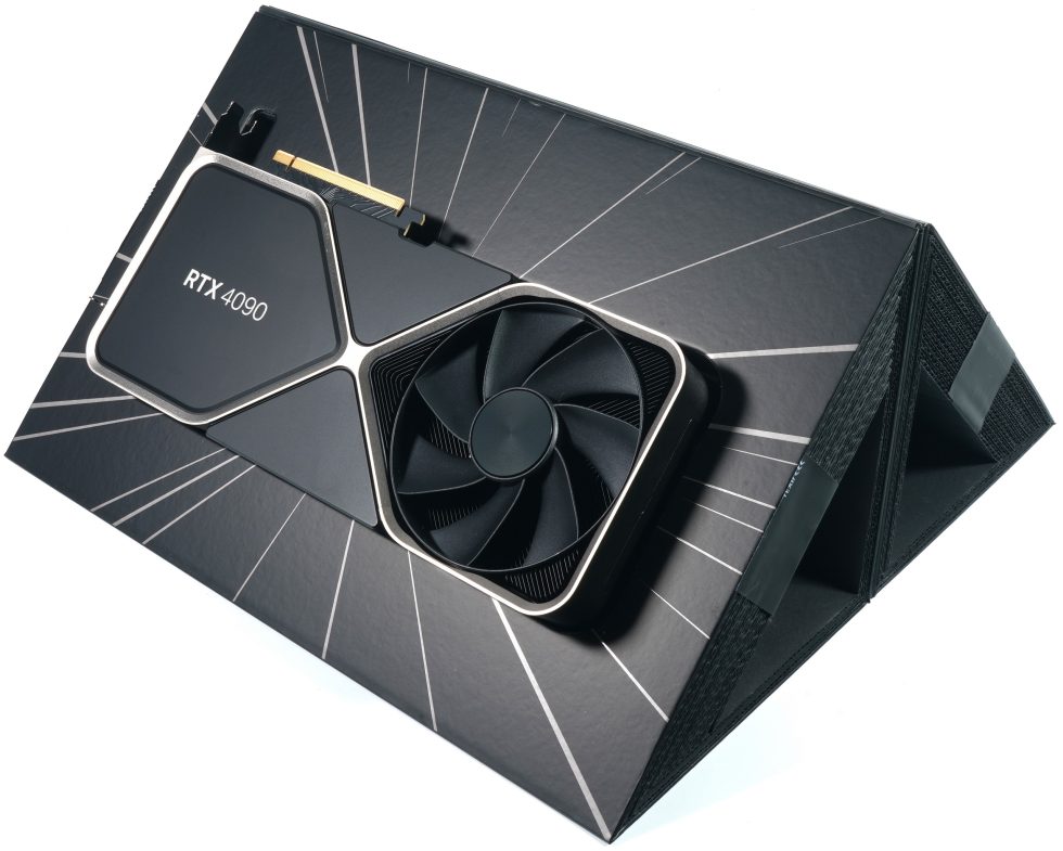
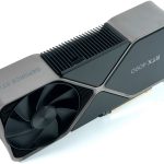
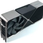
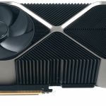
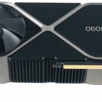
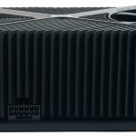
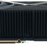
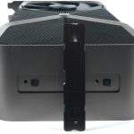
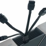
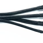
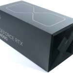
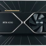
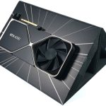
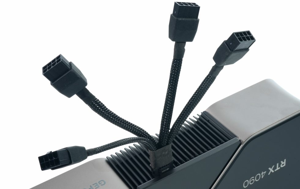
The FE weighs “only” 2075 grams. With the 30.5 cm length and 13 cm height from slot to top edge and a thickness of exactly 6 cm, this is still a real bruiser, but it is still significantly more compact than most board partner cards. With four 6+2 pin connectors, the included adapter to the 12+4 pin connector turns out to be much more powerful than the old triple of the GeForce RTX 3090 Ti. I wonder what awaits us in the final consequence? I know it already and you may be surprised right away!
And yet, it is enough to connect only three instead of four ports for the standard 450 watts that every card comes with ex-factory, because the card cannot control that. Or you can just use the cable provided by the power supply manufacturer, if there is one. Anyway, it looks funny how the four little screamers beg for electricity. Let them have it…
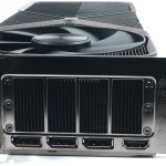
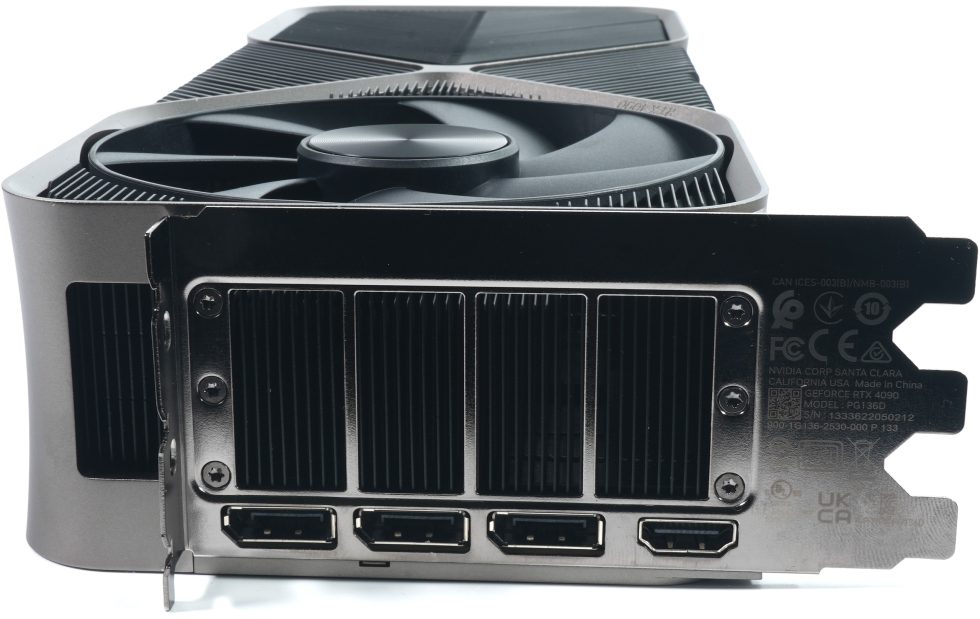
You can put not only power into the card, but also video connections. Four, to be exact, as there are: three times DisplayPort 1.4a and once HDMI 2.1a. That is especially a pity for the DisplayPort when it comes to the new specifications. Opportunity missed, unfortunately.
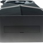
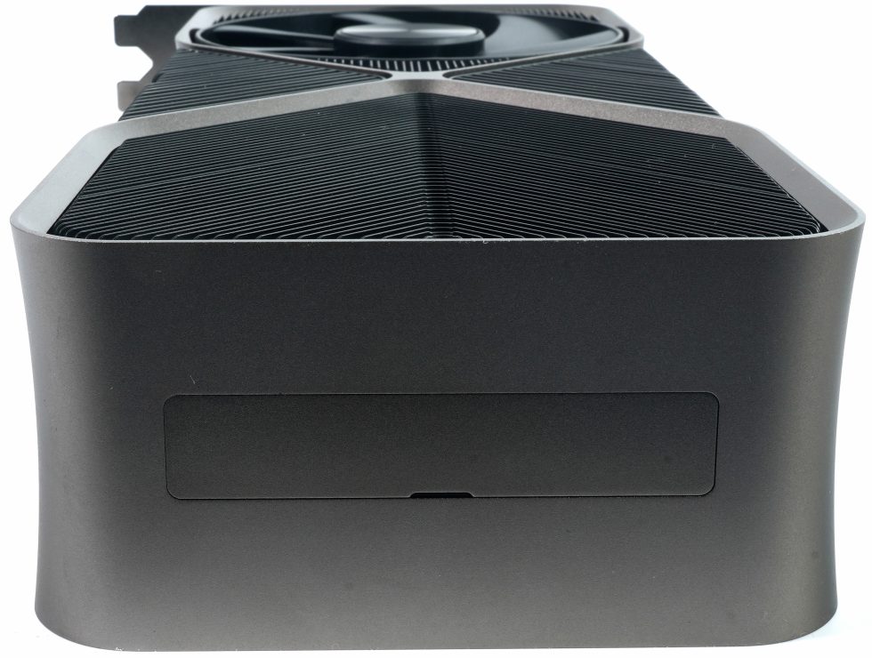
It looks like a closed event, but…
… it’s not the only magnetic clasp that you can unblade! But all in good time, today is the end of the underwear for now. Naked facts are coming soon, I promise!
 With that, the first page is done and we are slowly preparing for the test.
- 1 - Introduction, technical data and technology
- 2 - Test system in igor'sLAB MIFCOM-PC
- 3 - Teardown: PCB, components and cooler
- 4 - Gaming Performance WQHD (2560 x 1440 Pixels)
- 5 - Gaming Performance UHD (3840 x 2160 Pixels)
- 6 - Gaming Performance UHD + DLSS/FSR/XeSS (3840 x 2160 Pixels)
- 7 - DLSS 3.0 and the longest bars
- 8 - NVIDIA Reflex and Latency
- 9 - Workstation graphics and rendering
- 10 - Power consumption and load sharing
- 11 - Load peaks, capping and power supply recommendation
- 12 - Temperatures, clock rate, OC, fans and noise
- 13 - Summary and Conclusion









545 Antworten
Kommentar
Lade neue Kommentare
Urgestein
Veteran
Urgestein
Urgestein
Urgestein
Urgestein
Veteran
Urgestein
Veteran
Urgestein
Mitglied
Veteran
Urgestein
Veteran
Urgestein
Urgestein
Mitglied
Mitglied
Veteran
Alle Kommentare lesen unter igor´sLAB Community →