


Batch coding
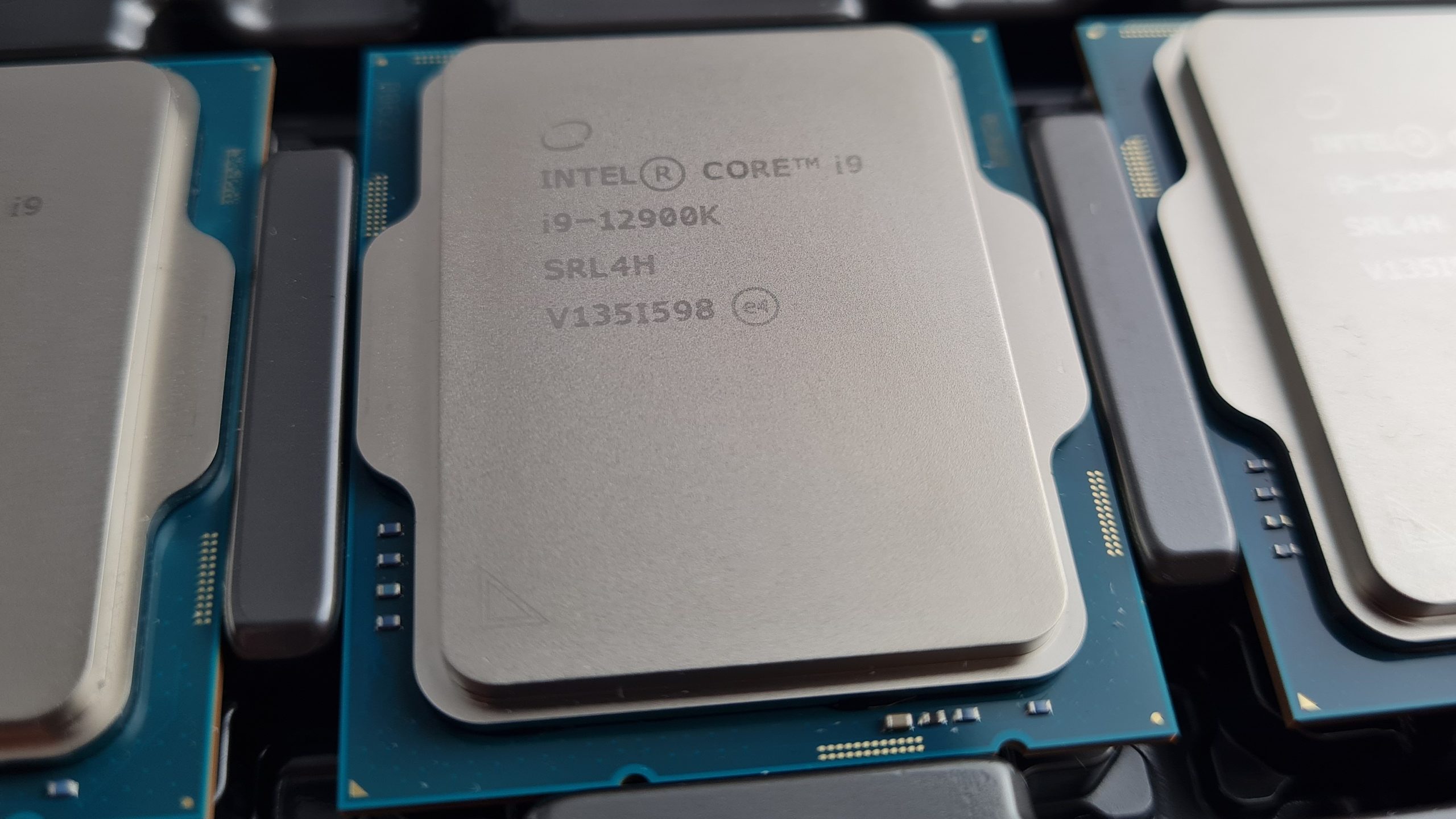
Two trays with 14 CPUs each were provided to us for the testing, one with i9-12900K and one with i9-12900KF (without iGPU) processors. The number of CPUs per tray has decreased from 21 since the last generation, which is probably due to the larger dimensions of the CPUs with the LGA1700 footprint.
Within a tray, all CPUs come from the same batch, i.e. production run. Intel’s batch numbers consist of a letter for the production location, 1 number for the production year, 2 numbers for the production week and a 4-digit alphanumeric counter. Thus, we can deduce that the CPUs from batch V135I598 are made in China in the 35th week of the year 2021. Accordingly V134K380 means one week earlier. By the way, I also included my two i9 “boxed” CPUs, which I bought privately at launch, in the statistics, although they are also a V134 batch.
For comparison, a majority of the CPUs tested by quiekMew and colleagues start with X, which means production location Vietnam. Then again, the production period overlaps with weeks 31, 35 and 36 from 2021 with the chips I have binned.
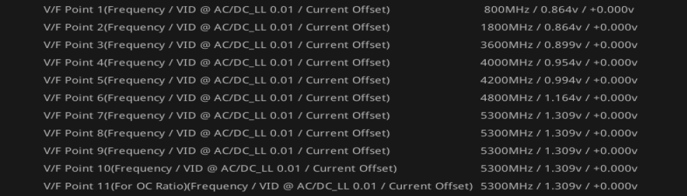
There is another interesting side observation to mention about the V/F points. Because while the KF CPUs manufactured in week 34 have a V/F point 7 at 5.2 GHz, which is also the Intel spec, the K CPUs from week 35 have the same point at 5.3 GHz, which is 100 MHz higher. Intel might have originally designed Alder Lake with Thermal Velocity Boost, but then deactivated it shortly before the market launch. I wonder if the planning of the upcoming KS-SKU might have something to do with this?
Test methodology and hardware
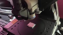
Now the actual task was to find a CPU with the highest possible quality memory controller (IMC) for DDR5 tests. Exactly here, the motherboard also plays a, if not the leading role, when it comes to pushing the clock limit. So it couldn’t have been more fitting that overclocker safedisk from the Asus R&D team recently sent us a hand-selected Maximus Z690 Apex motherboard. So at this point, many thanks to Asus and safedisk for the motherboard!
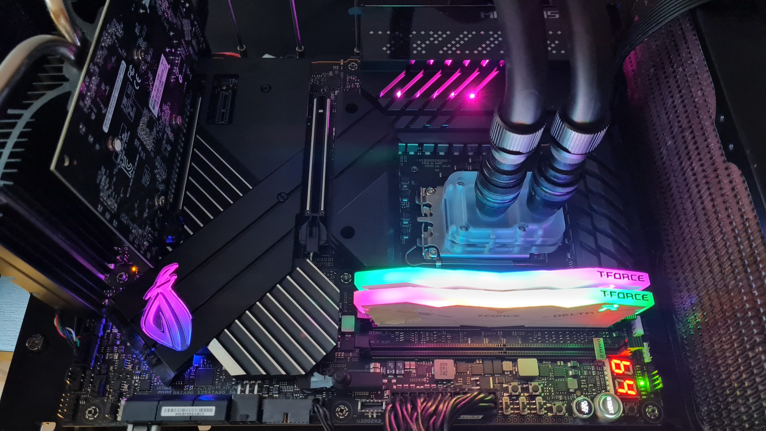
By the way, the dedicated review of the motherboard with differences to retail samples will be available next week and should not be missed either. Hynix 16 Gbit M-Die based UD5-6400 modules from Teamgroup are used as RAM. However, their quality is only secondary for now, since I don’t test for complete stability in my IMC binning – also because it wouldn’t be feasible in terms of time – but only determine the highest clock frequency with which it is still possible to boot into Windows and open HWInfo.
On the one hand, this is fast, but on the other hand, it also shows whether a few simple memory operations can be performed largely without errors. And you might be surprised how big the differences between the CPUs are already here. Speaking of surprise, DDR4 binning with an MSI Pro Z690-A and Samsung 8 Gbit B-Die modules from G.Skill is also done for comparison. I was also interested in whether the clock potential of the IMCs can be transferred from DDR5 to DDR4 and vice versa. All DDR5 and DDR4 tests are run in dual-channel mode, with two single-rank modules each. For simplification, the two dedicated IMCs of Alder Lake CPUs are called in the singular as “IMC” in the following. As always, a complete listing of the hardware can be found here:
|
Test systems |
|
|---|---|
| Hardware: |
|
| Cooling: |
|
| Housing: |
|
| Periphery: |
|
| Measuring devices: |
|


21 Antworten
Kommentar
Lade neue Kommentare
Veteran
Urgestein
Veteran
Mitglied
1
Mitglied
1
Urgestein
Mitglied
Neuling
Mitglied
Urgestein
Urgestein
Mitglied
Urgestein
Veteran
Urgestein
Veteran
Veteran
Alle Kommentare lesen unter igor´sLAB Community →