


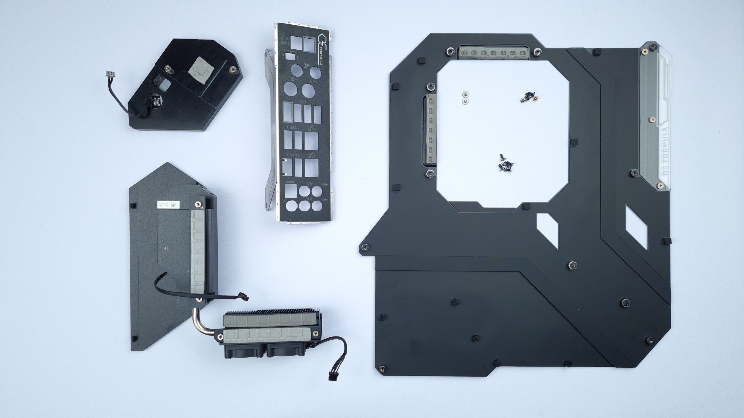
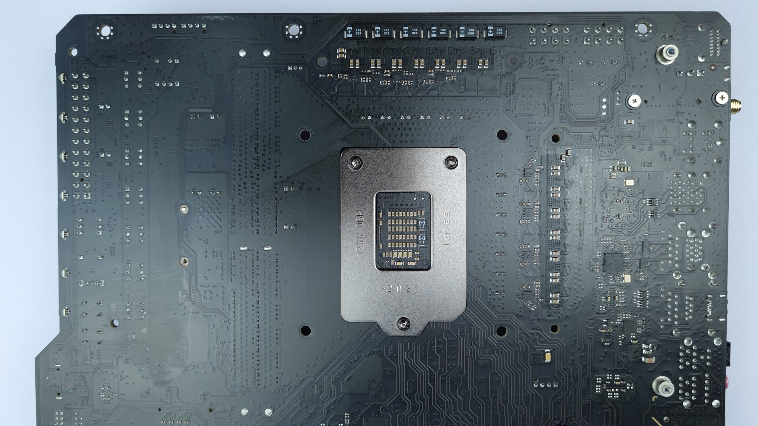
The disassembly of the backplate and various heatsinks is simpler than with some graphics cards. 5 PH1 Phillips screws on the front and 6 on the back must be loosened to remove the sandwich of heatsink, PCB and backplate. The backplate is covered with a black foil on the bottom side to isolate the conductive aluminium from the board in any case.
Both backplate and heatsinks are equipped with 1.5mm thermal pads. One half of the Vcore VRM even cools the coils, while the other half is exposed. Two more PH1 Phillips screws now only fix the IO shield to the board, where the IO heatsink also hooks into.
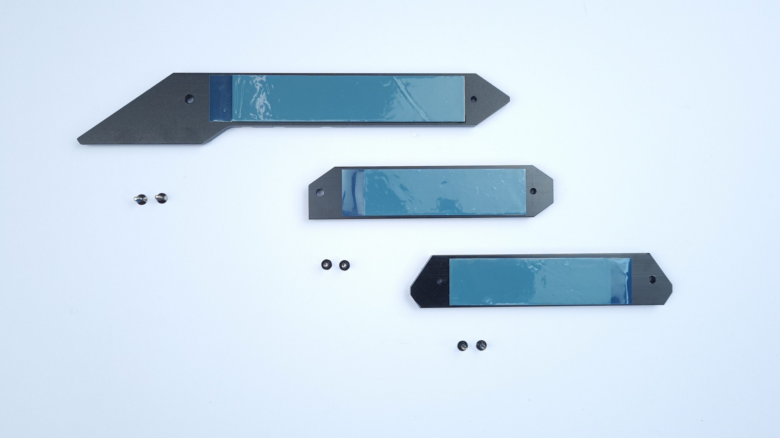
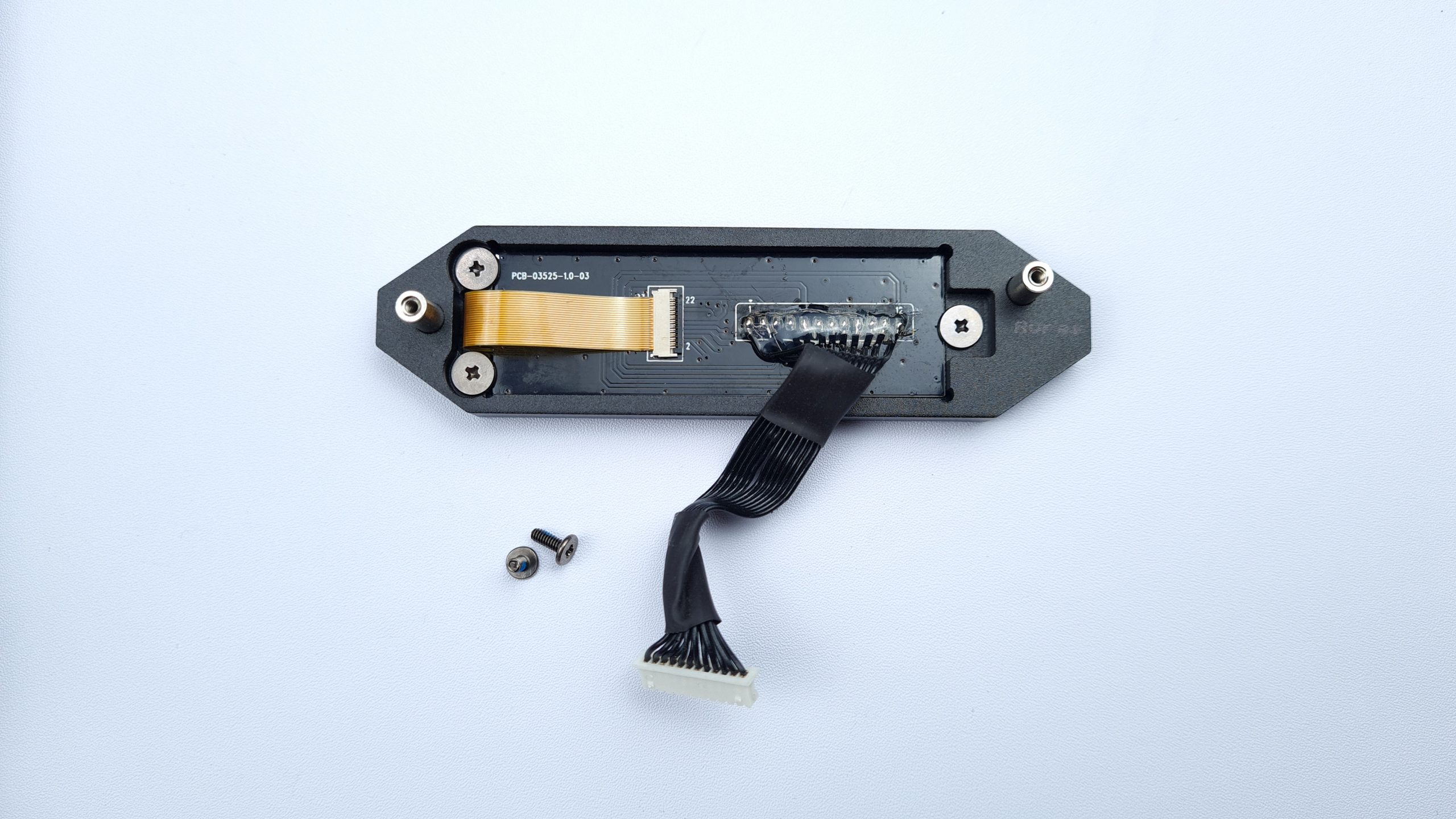
Now only the OLED display remains, which is also mounted with 2 more PH0 Phillips screws, and the 3 M.2 heatsinks with their 2 Torx T9 screws each, for which a suitable screwdriver is included. What an easy and uncomplicated disassembly, thanks ASRock!
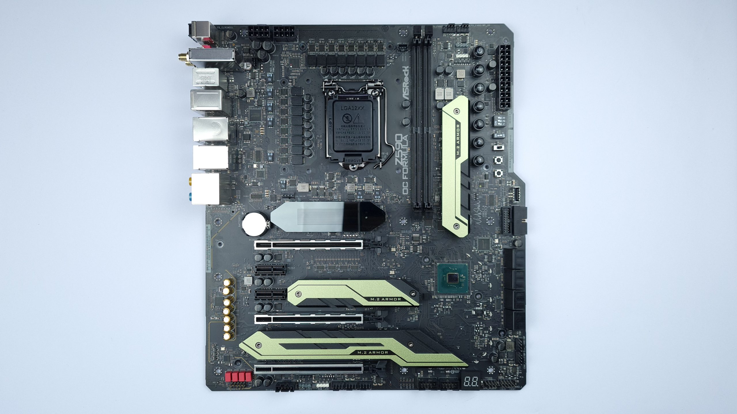
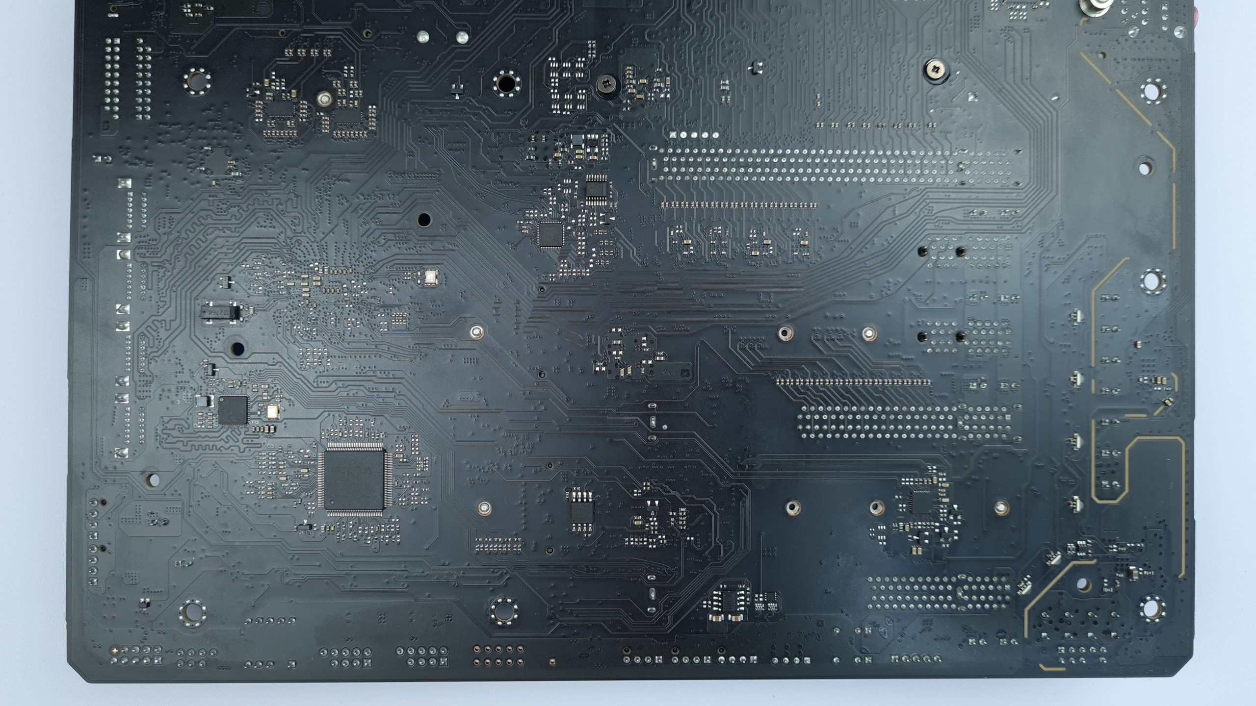
All that’s left is the bare PCB in eATX format, which extends another 30mm from the center of the right ATX screw points. We will take a closer look at the components that are permanently installed on it in a moment. But before we go into too much detail, let’s take the opportunity to look at the rest of the board’s connections.
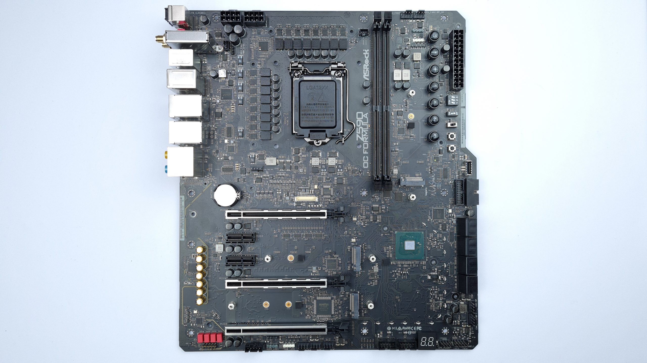
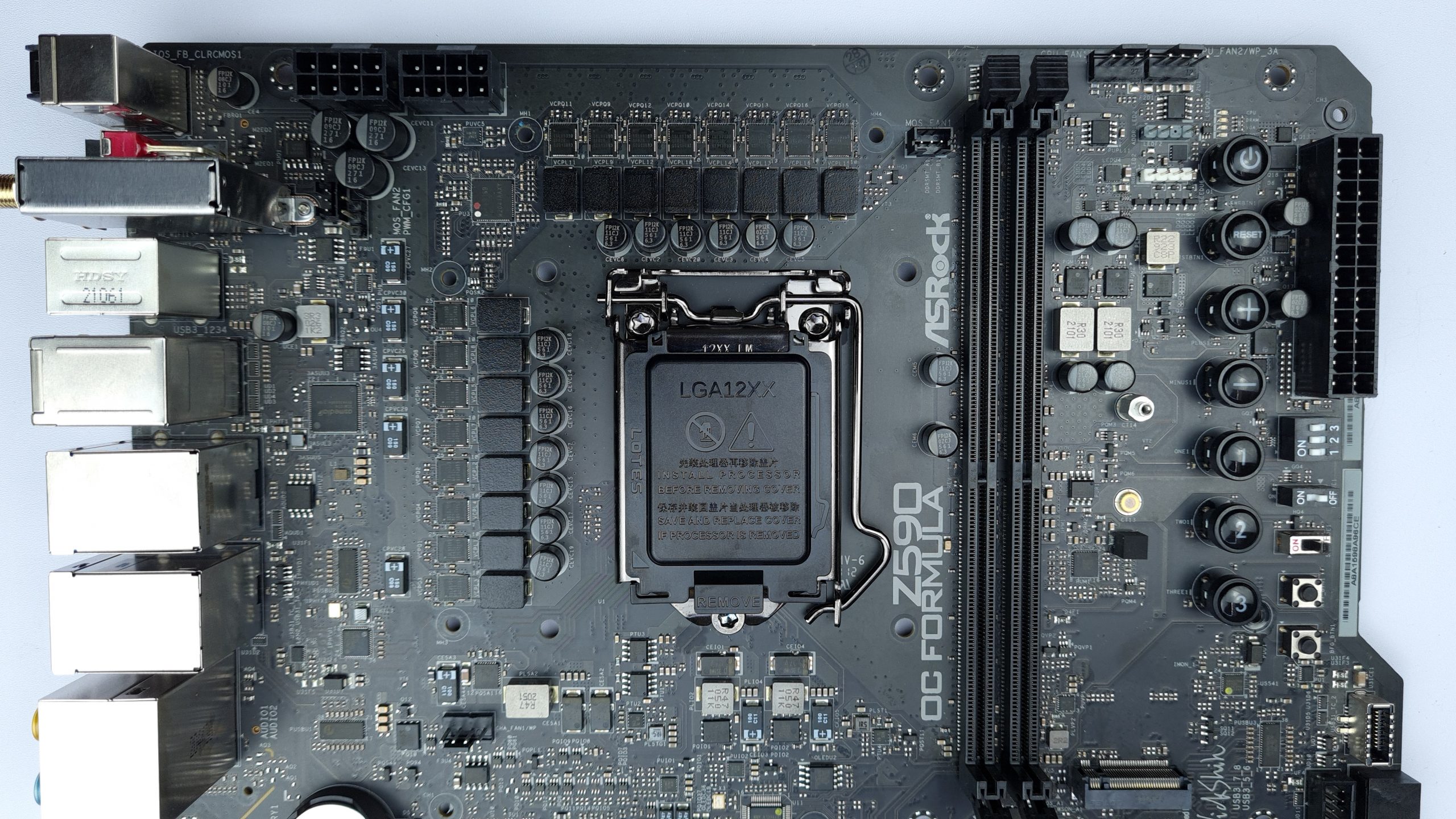
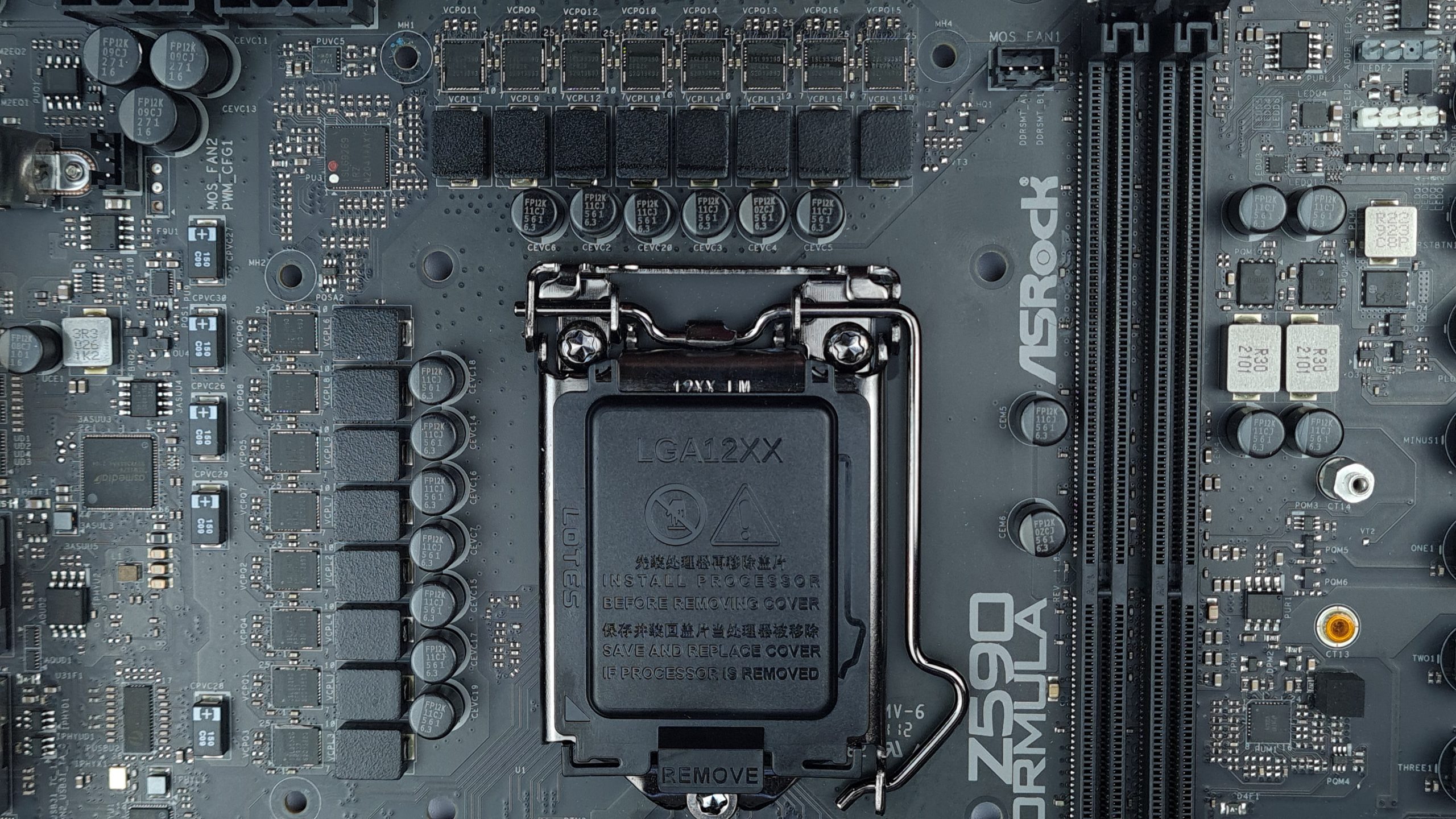
The 24-pin ATX connector has slid up unusually far to make room for the buttons, but that shouldn’t be much of a problem for cable routing. Further power is supplied by 2 8-pin EPS connectors in the upper left corner of the board. Also, in the upper half of the board we find two 4-pin fan connectors on the top right and another one in the middle near the IO, one 3- and 4-pin RGB header each, as well as an 80 mm M.2 slot between DIMM slots and 24-pin connector. Also, on the right edge of the board you’ll find all the buttons and switches, as well as an internal USB 3.2 Gen2 20 Gbit/s port for the case.
In the top left near the power connector for MOS fan 2 there even are soldering pads for an I2C header, through which you can talk to the pwm controller directly, if you are able and willing to. The header you see in the picture was installed by me before taking the photos. As mentioned, from the factory there are only 3 soldering pads.
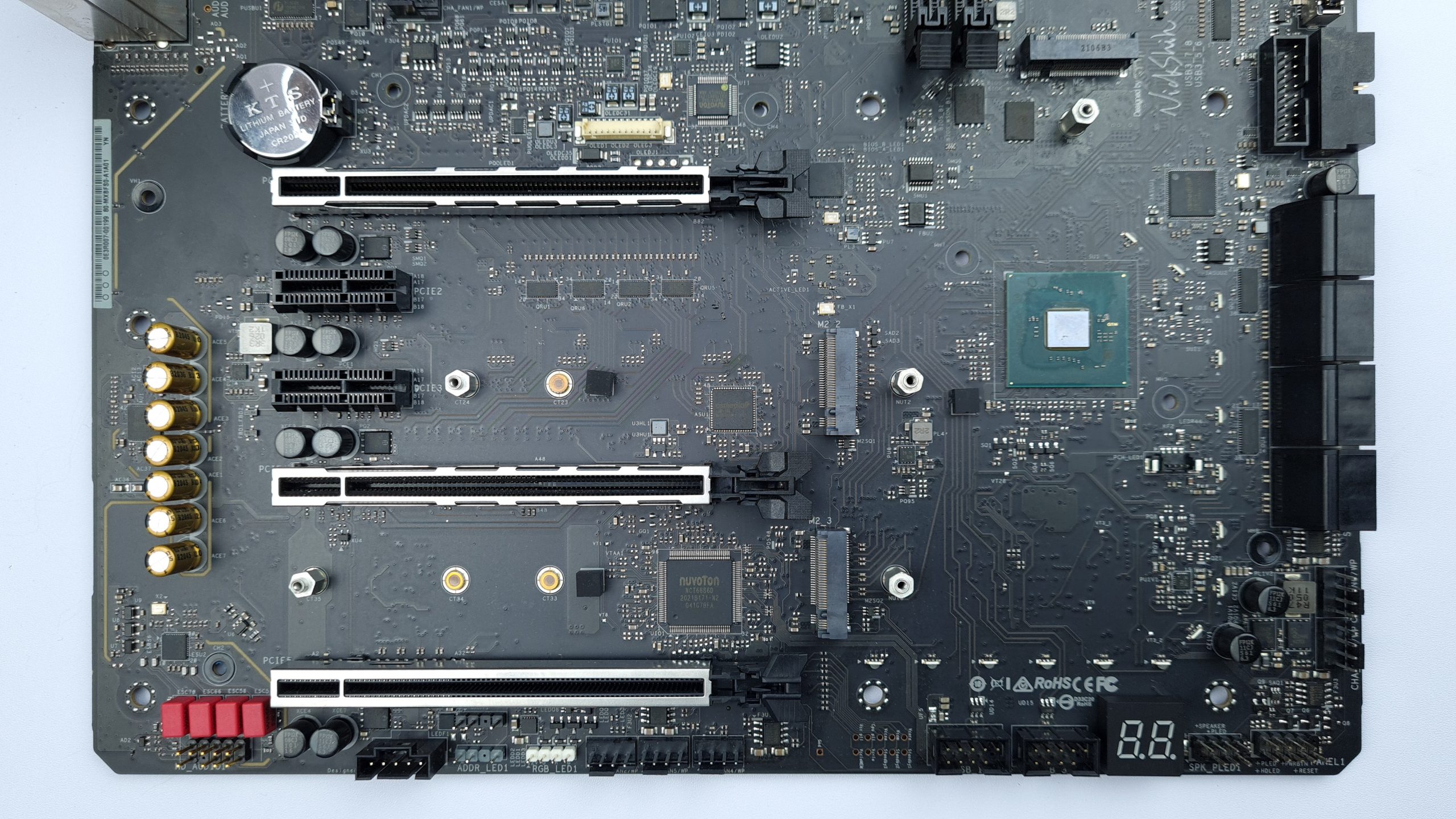
In the bottom half, the three PCI-E x16 slots stand out first, electrically connected x16, x8, x4 from top to bottom, with the last running at Gen 3 through the chipset rather than the CPU. The top two are running in either Gen 4 or Gen 3, depending on if a Rocket Lake or Comet Lake CPU is installed. In between there are two open PCI-E 2.0 x1 slots and two M.2 slots with 80 and 110 mm length respectively. On the bottom edge you’ll find the usual connectors for HD audio, a Thunderbolt AIC connector, another 3- and 4-pin RGB header each, 4 more 4-pin fan connectors, voltage measurement points, two USB 2.0 headers, the postcode display, and speaker and front panel connectors.
On the right edge, you’ll find two internal USB 3.2 Gen1s, one of which is angled at 90 degrees. 8 SATA 6 Gbit/s ports, 6 of which are powered by the Z590 chipset and 2 by an ASMedia ASM1061. Finally, there are now 2 more 4-pin fan connectors underneath. The CMOS battery as well as the connector for the OLED display are located above the first PCI-E Express slot and therefore offer good maintenance or visibility.
Even though the Z590 OC Formula is explicitly advertised as an extremely OC-focused motherboard, it is also perfectly suited for a gaming or workstation system with a strong focus on performance with this firework of connectivity.
How many VRM phases? – Yes.
A closer look at the installed components quickly reveals ASRock’s advertised 16 phases for the core voltage supply in an L-shape around the CPU socket. And yes, all those phases are actually just for Vcore, which is the voltage for the CPU cores and cache.
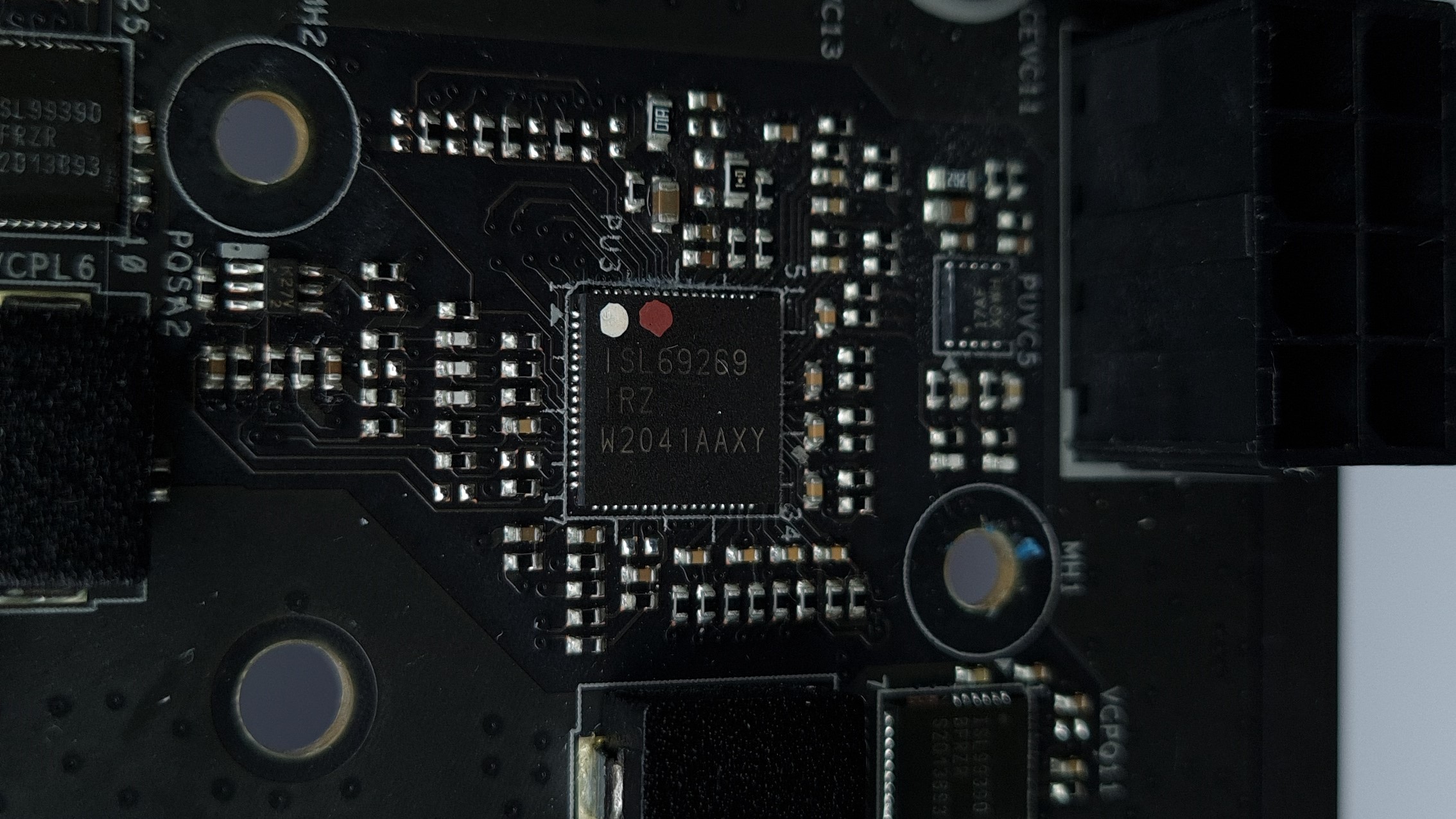
ISL99390 Smart Power Stages from Renesas, specified for 90 A each, are used for this purpose. They are controlled by an ISL69269 12-phase PWM controller, also from Renesas. How do you get from 16 to 12 phases? We’ll get to that in a minute, but it’s definitely going to be interesting.
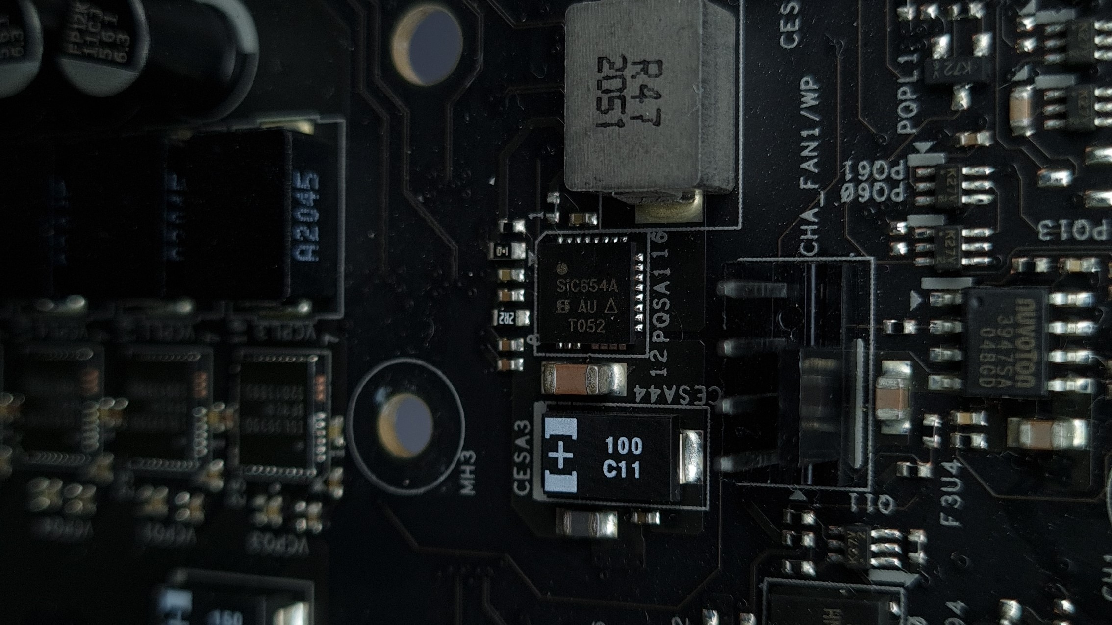
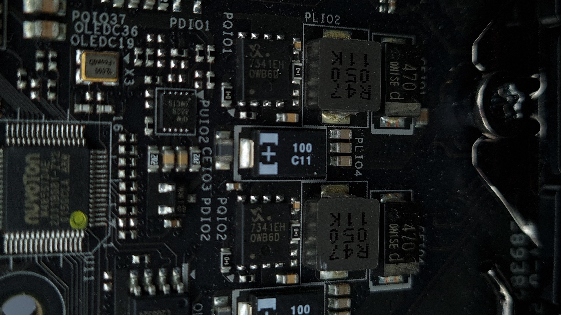
The other three small voltages for the CPU each have a single phase below the socket. The system agent voltage is supplied by a SiC654A Dr. MOS component from Vishay, specified for 50 A. The two IO voltages, IO and IO Mem are each supplied by a 7341EH 24 A MOSFET from Sinopower.
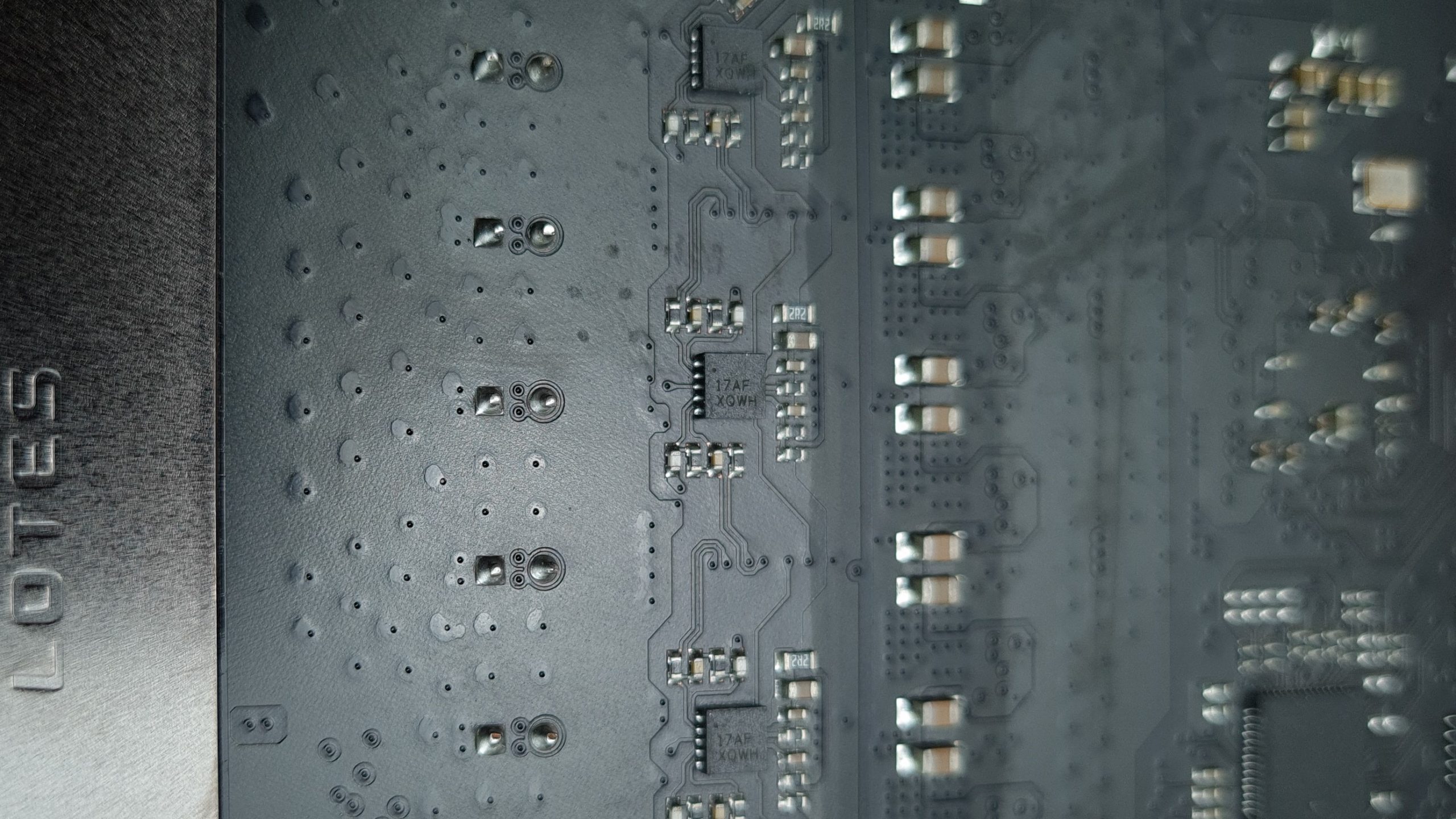
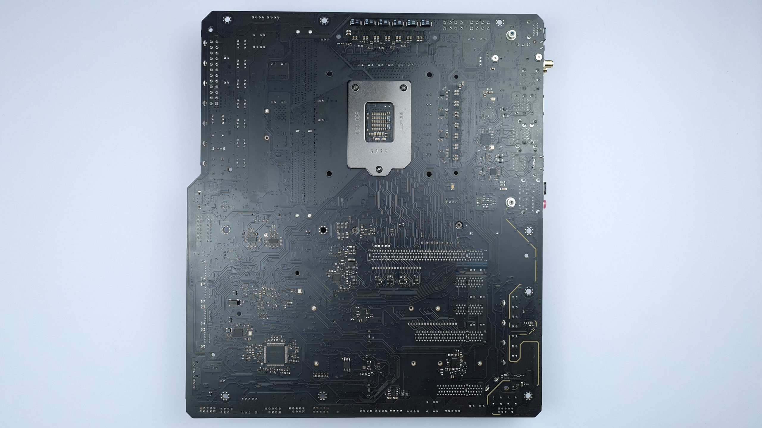
To solve the puzzle of the layout of the various CPU voltages, we have to look at the backside of the board, where 7 ISL6617A PWM couplers are located. But how do 7 doubles fit to 16 phases of core voltage? Actually there is anohter, 8th ISL6617A on the front, just below the 8-pin EPS connectors. Now that seems a lot more logical.
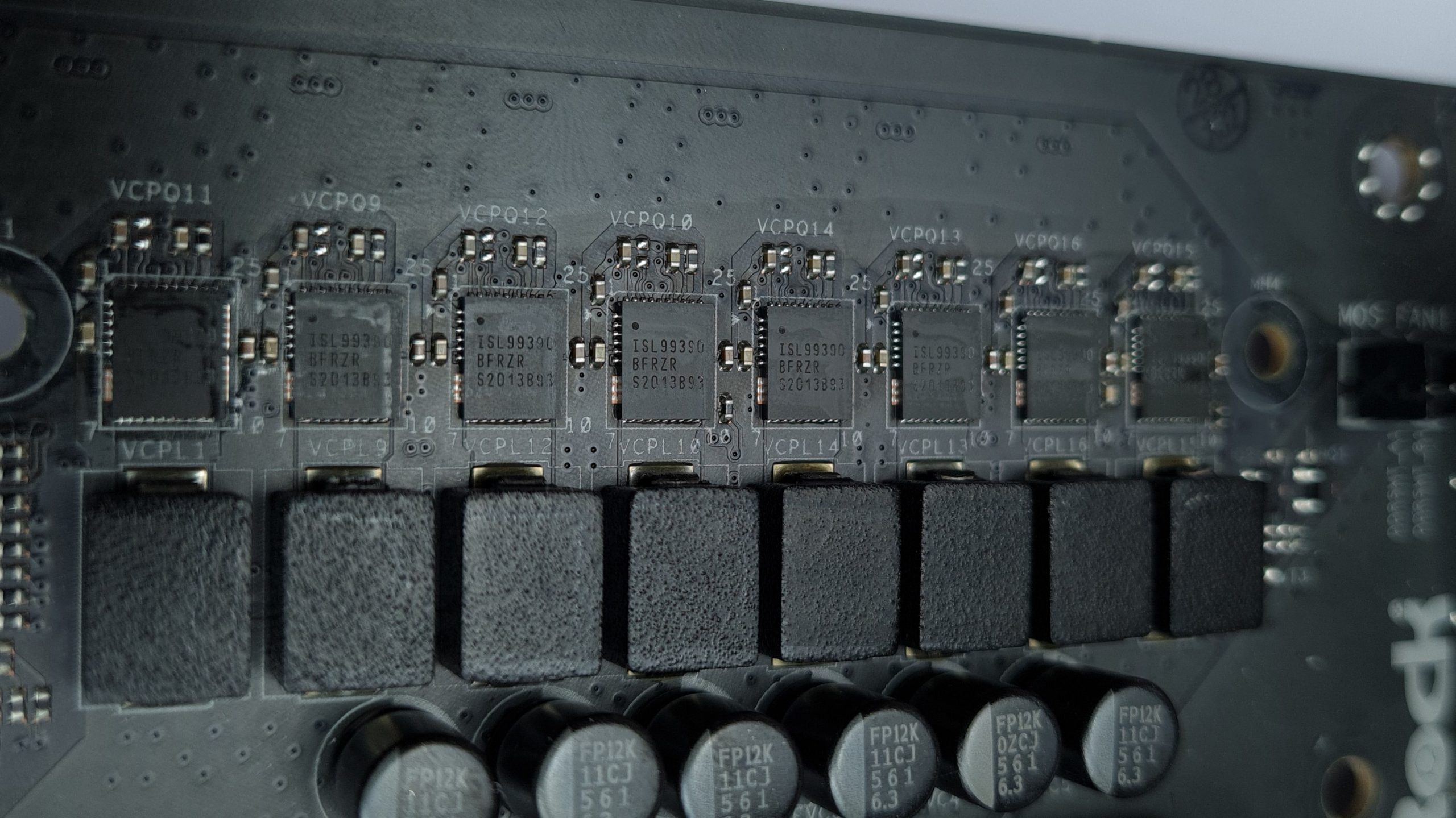
So the CPU core voltage is supplied by the ISL69269 with 8 real phases, which are then doubled, i.e. 8 * 2 = 16. Then the PWM controller still has 3 phases free, with which it only supplies SA. IO and IO Mem have their own dedicated APW8828 single-phase PWM-Controllers from Anpec. So the ISL69269 is effectively only operating in 9 phase-mode. ASRock thus takes full advantage of the individual streghths of the VRM components and thus enables a high-quality and relatively cost-effective voltage supply at the same time. Thanks to asdkj1740 on the forums for the correction and insight!
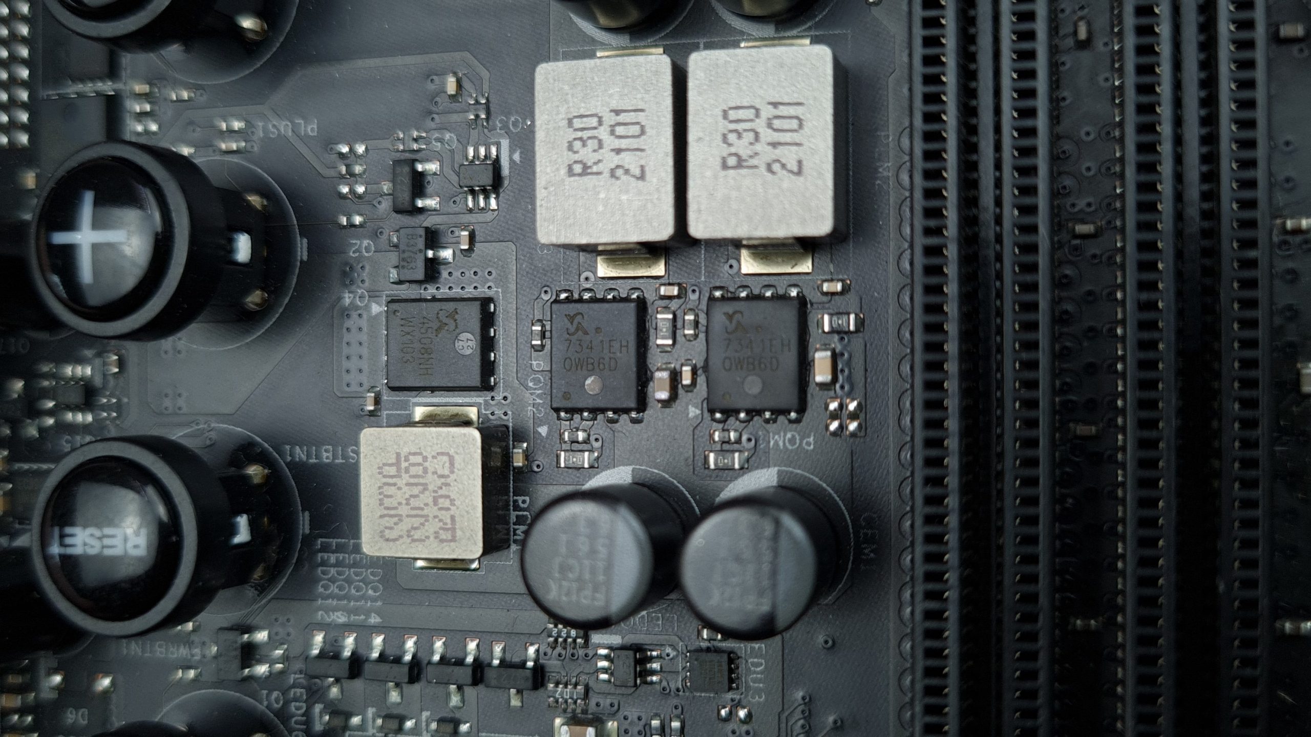
The two phases for the voltage supply of the DIMM slots should not remain unmentioned, for which also 2 7341EH 24 A MOSFETs from Sinopower are used, controlled by a dedicated PWM controller, a uP1674p from UPI Semiconductors, which is also more than enough for 2 DDR4 DIMM slots and should not be a limit under any circumstances.
When it comes to the VRM of the Z590 OC Formula, ASRock has really brought out all the heavy guns that can be bought and installed. Whether you actually have to call up all this potential power in one case, I dare to doubt, but there are the reserves in any case. And especially in extreme overclocking, where hundreds of variables have to be perfectly matched for the best results, you definitely don’t have to worry about the voltage supply anymore with this board.


11 Antworten
Kommentar
Lade neue Kommentare
Veteran
Mitglied
Veteran
Moderator
Neuling
Urgestein
Veteran
Urgestein
Neuling
Mitglied
Alle Kommentare lesen unter igor´sLAB Community →