


My sincere thanks go in the first place of course again to one of my industry partners, where they selflessly and in their free time realized the appropriate investigations and also the necessary technical preliminary work. In addition, we also provide technical advice and practical implementation of the tests, which are somewhat alien to the industry. Unfortunately, we cannot and are not allowed to offer you original pictures from the lab for understandable reasons of secrecy in such areas, but the product pictures certainly do.
However, we are not a science magazine here, but want to reach as broad a mass as possible and also convey some background knowledge without the reader despairing at the very first paragraph. That’s why I had to break the following down very far, but I hope that it will be more understandable this way and that the experts will forgive me anyway. It is rather explained in a popular scientific way, but there is no other way here.
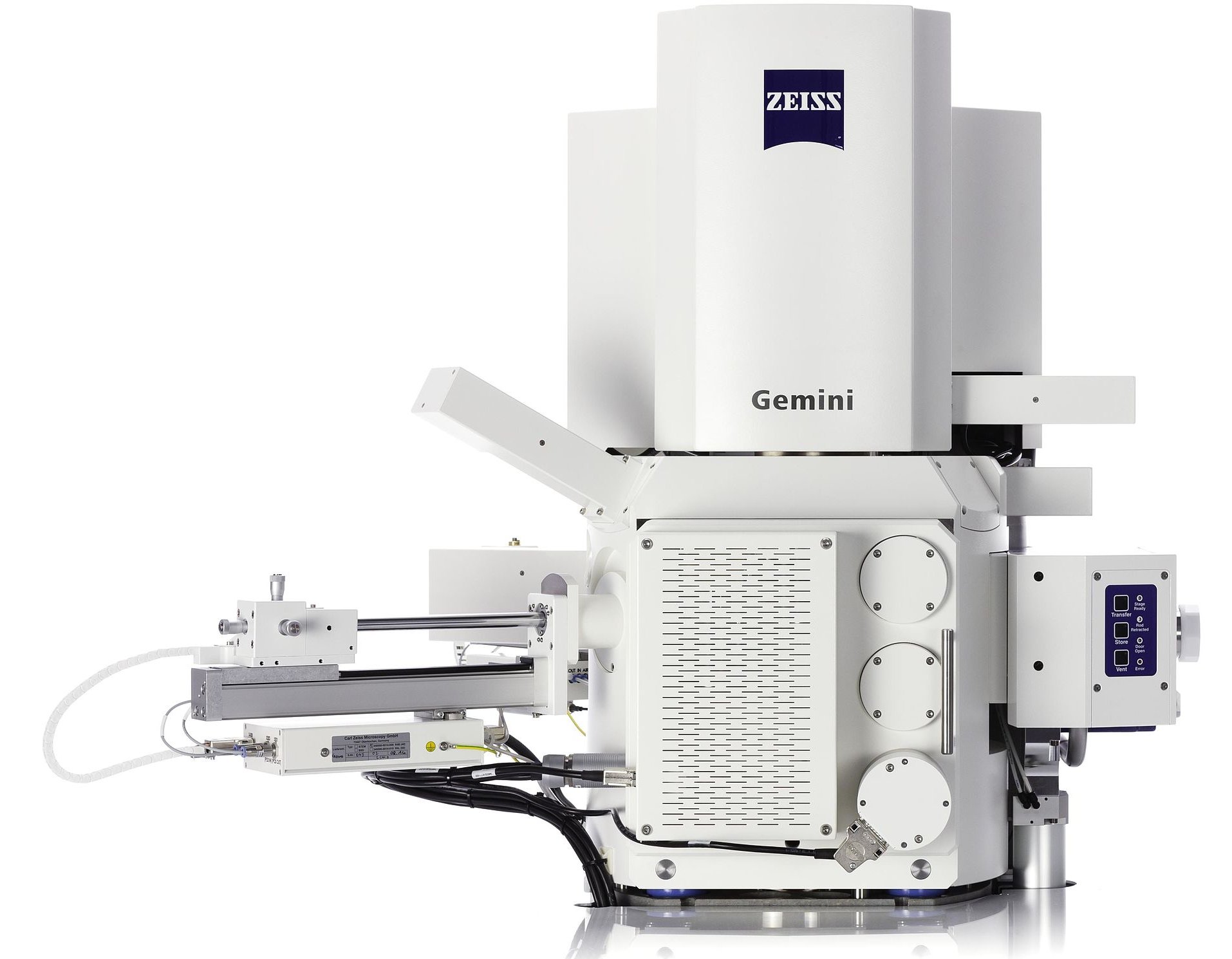
Scanning Electron Microscope (SEM)
For the sake of simplicity, I’ll stick with SEM, although the German substitution REM (for scanning electron microscope) is, after all, synonymous. But since these abbreviations also appear in the product names, I’d better leave it at the original. I will leave aside the different ways of image generation like resting or scanning electron microscopy, as well as the realization via transmission (TEM, STEM) or backscattering (SEM), since we primarily rely on a reflection microscope and some of the methods may even overlap. Basically, it is a complex electron optics system in which a combination of electromagnetic and electrostatic lenses guides a fine electron beam as a raster over the rectangular object area to be tested. The final image is created by the synchronous registration of a signal triggered or influenced by the electron beam.
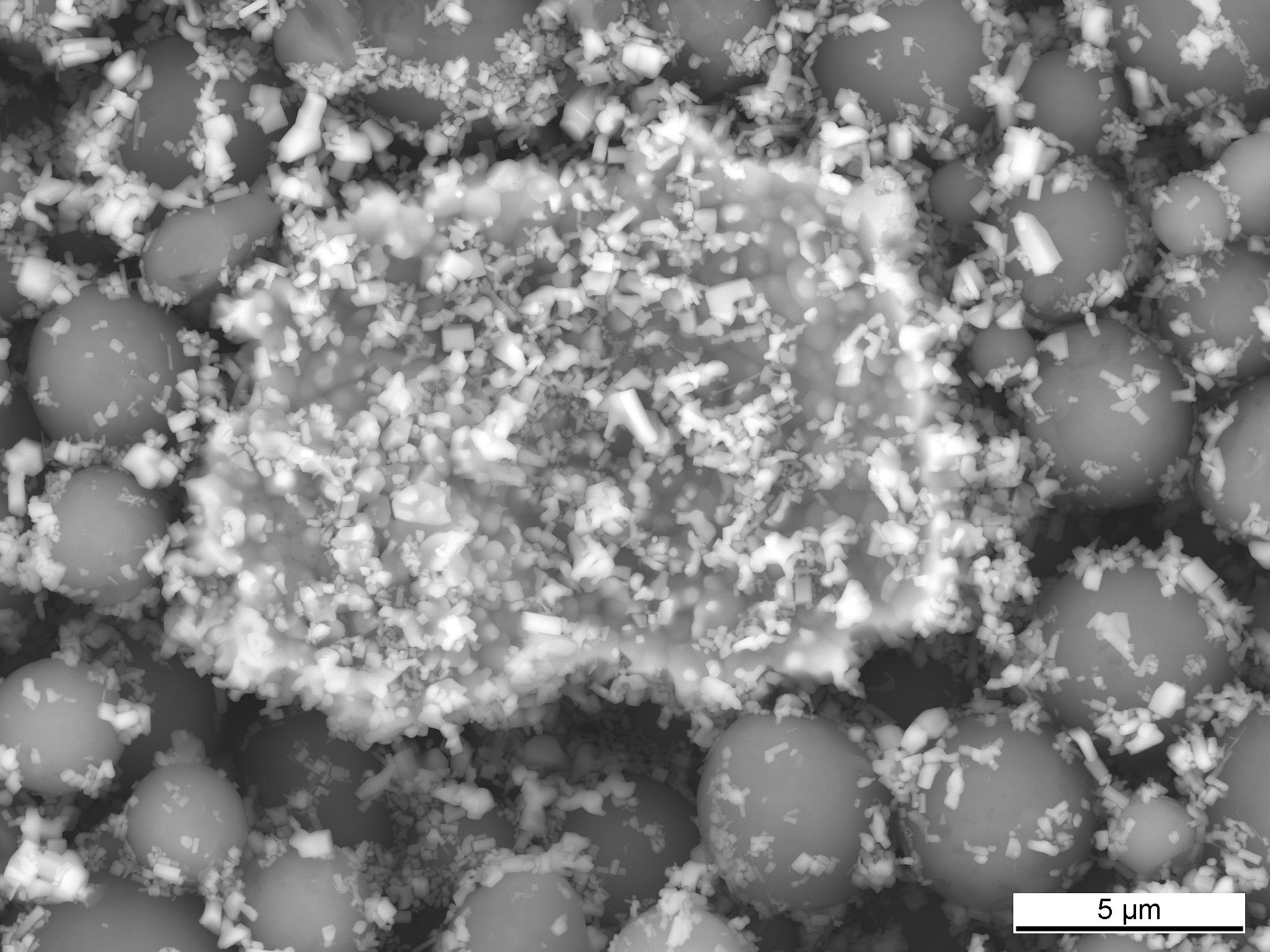
There are methods that rely primarily on the secondary electrons (SE), but we are most interested in the backscattered electrons (BE or BSE), and the image of the MX-4 above shows the BE contrasted very nicely. To explain, these BEs are those electrons from the primary beam which are then elastically scattered at the hit atomic nuclei in the nanometer range below the object surface. The amount of backscattered electrons is directly related to the average atomic number of the material under study.
Here in the picture we see the comparison of ZnO to Al. The heavier ZnO has much more electrons in the shells than Al. Thus, there is a greater probability of backscattering of primary electrons. As a result, more signals arrive at the detector. Thus, the backscatter signal already provides chemical information: the parts that appear brighter in the image have a higher average atomic number than the parts that appear darker. Otherwise, of course, the following also applies: Deeper areas of the special object appear darker, the closer ones bright, resulting in a plastic and quite contrasty image.
The measurable energy of these electrons is in the range of the irradiated primary electrons and the resulting image resolution (depending on the primary energy used) is in the micrometer range. With the help of electron backscatter diffraction (what a word), the crystallographic orientation of the crystals on a surface could also be used to determine certain material properties, but that would really be going a bit too far now.
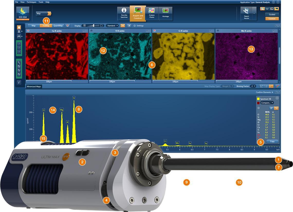
But we also need another tool for our final analysis. After all, we still have to enable the scanning electron microscope used to perform special chemical analyses on the surfaces in the micrometer range. For this purpose, we use energy dispersive X-ray analysis (EDX). By combining the SEM imaging raster process with EDX, it is also possible to capture beautiful elemental distribution images (top image). For EDX, the atoms are excited by an electron beam with a very specific energy, which in turn results in X-rays with an energy characteristic of the element in question. The resulting emission is therefore used to obtain information about the composition of the thermal paste.
Of course, the whole thing is now described very simplified, but so completely I can not spare you unfortunately. But I can reassure you, because from the next page on, also because you have held out so bravely until here, it will be easier and also more entertaining. So that the aforementioned silicone oil does not bother us, we will virtually “wash” the paste in the first work step. Please turn the page once!


42 Antworten
Kommentar
Lade neue Kommentare
Urgestein
Urgestein
1
Veteran
Veteran
Veteran
Veteran
Veteran
Veteran
Urgestein
Urgestein
Urgestein
Urgestein
1
Veteran
Urgestein
Mitglied
Veteran
Urgestein
Alle Kommentare lesen unter igor´sLAB Community →