


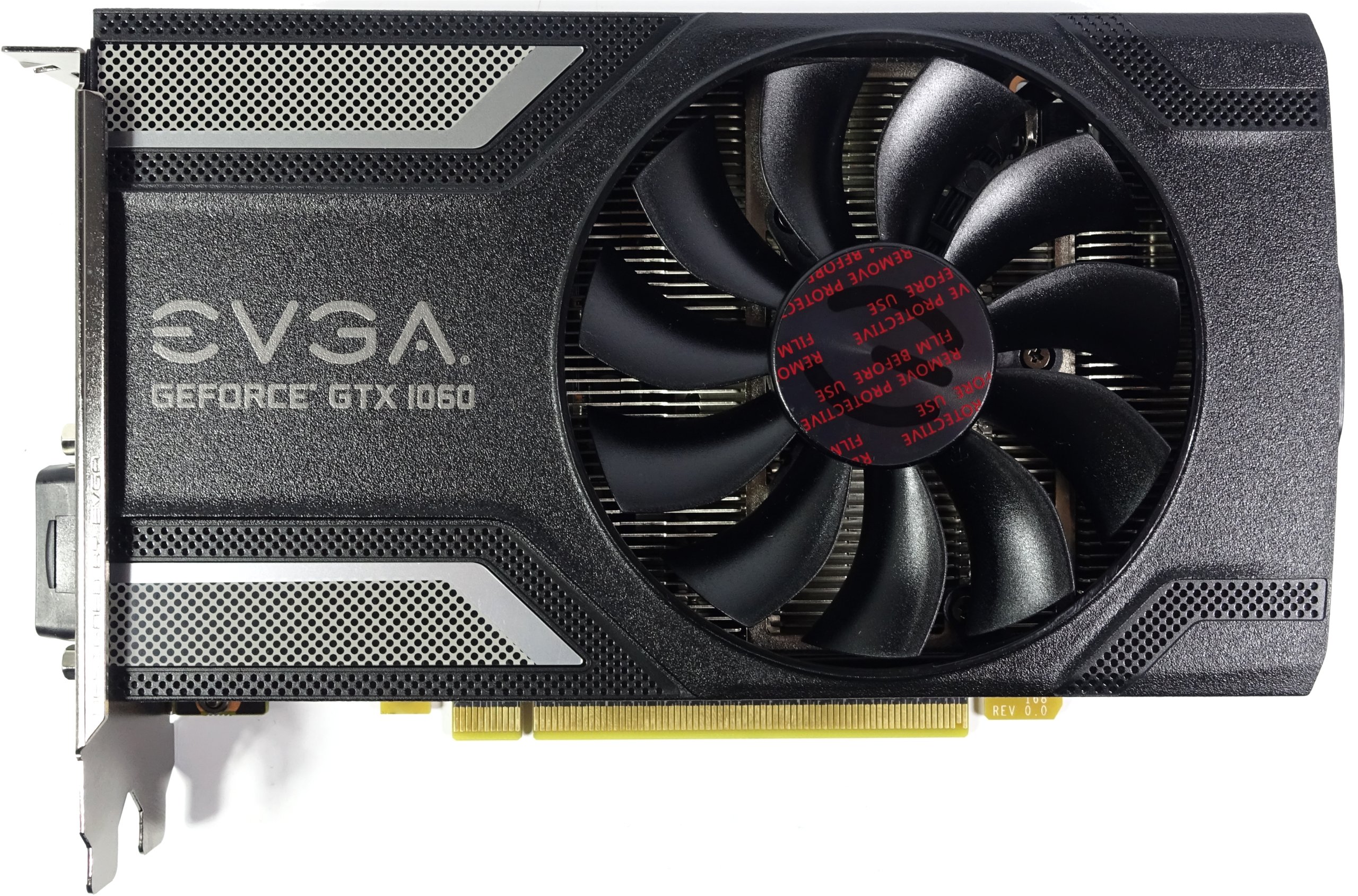
 With the GeForce GTX 1060 Superclocked (6GB), EVGA has a GeForce GTX 1060 in its portfolio that roughly relies on Nvidia's reference board, but which interprets the cooler in such a way that there are no overhangs like the Founders Edition.
This creates a rather short and crisp map, which at first glance is almost obvious for projects such as HTPCs. But can the card ultimately keep what it promises at first glance? We want to examine exactly to what extent the cooling solution is sufficient for this.

But there is one thing we need to do: the current model has some minor vulnerabilities, which we have already discussed in detail with EVGA. For example, the current BIOS will be revised again and later – after verification by Nvidia – will also be offered for download online. Our measurements were made with the downloadable version at the time of the test (86.06.0E.00.16).
UPDATE: EVGA has announced a change to the BIOS and is also reviewing our proposals to improve VRM cooling.
However, since EVGA explicitly allows the cooler change, any interested user can do our mod with just a few simple steps without losing the warranty.
We will update this information as new facts emerge.
External structure and connections
The radiator cover is made of simple, anthracite-grey plastic and dispenses with any optical frills except for two simpler plastic applications. This may well please, because especially in very small cases you won't see the map anyway. "Useful" and "favourable" are also interesting attributes.
With a length of 18.4 cm from slot aperture, 10.5 cm installation height from the top of the motherboard slot and 3.5 cm of installation depth, the EVGA GeForce GTX 1060 Superclocked with its 576 grams presents itself almost as a lightweight dwarf. By the way, if the space becomes too narrow, the cover could easily be shortened manually by another eight millimeters in length – provided that the tool and skill are.
 |
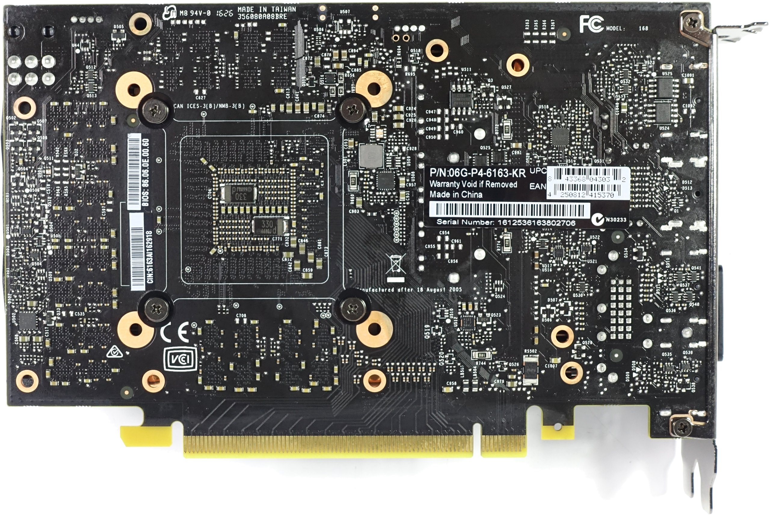 |
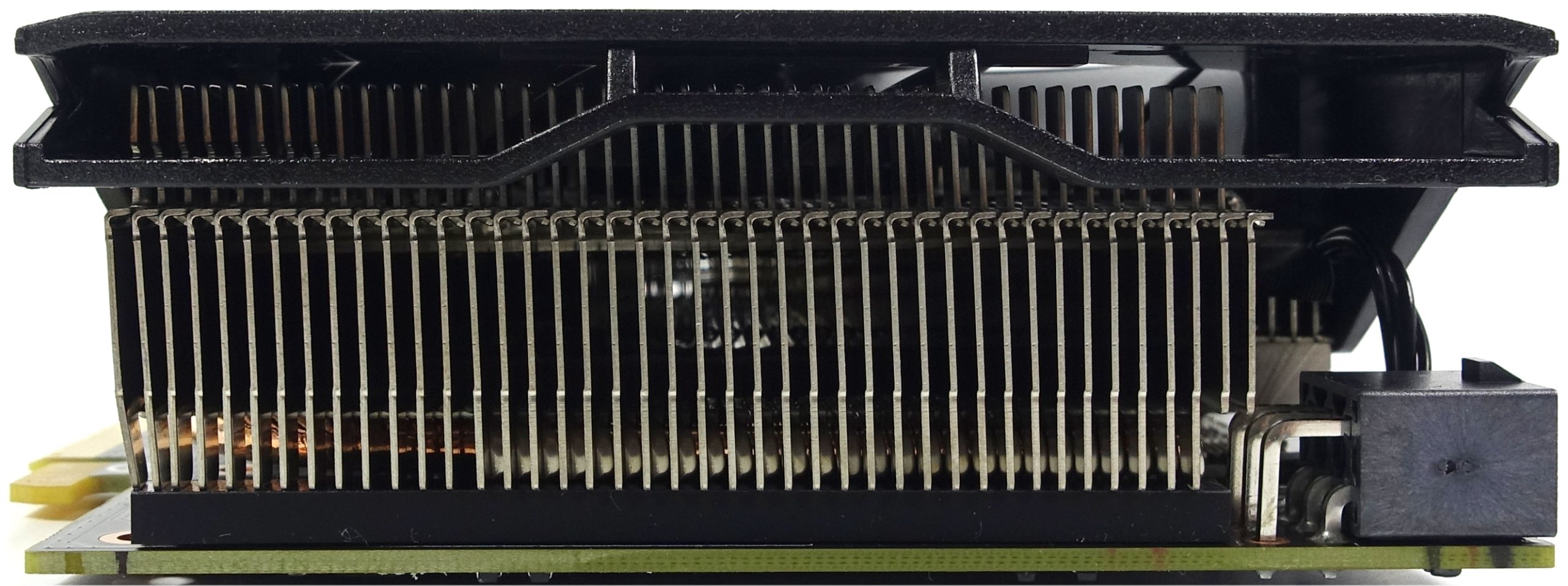
EvGA has also dispensed with the backplate for cost reasons, which makes it even more interesting for mini-ITX boards. This leaves around five millimetres more space for the CPU cooler, which often decides enough about the success or mismanagement of such a combination.
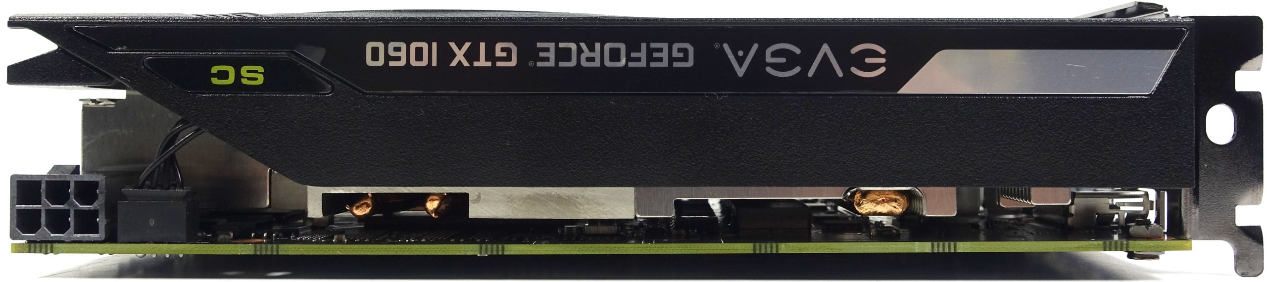
The top of the card bears the EVGA lettering on the type label, but you can't find RGB lighting. The reasons are well known and understandable. The simple 6-pin connector sits at the end of the card and is not rotated.
A closer look at the two heatpipes on the ground shows us that, despite the compact design, we are relying on a heatpipe solution, which we will discuss in more detail later. even need to.
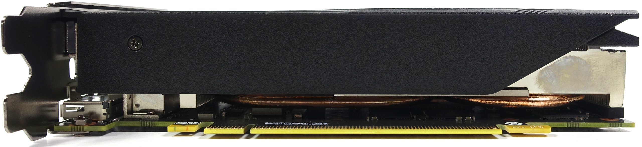
The horizontal slat alignment ensures that a not inconsiderable part of the waste heat is carried out of the housing via the very air-permeable slot aperture thanks to the many openings. You can see this principle of air flow at the end of the map, but here the air lands in the middle of the housing, which makes a good airflow all the more important.
 |
 |
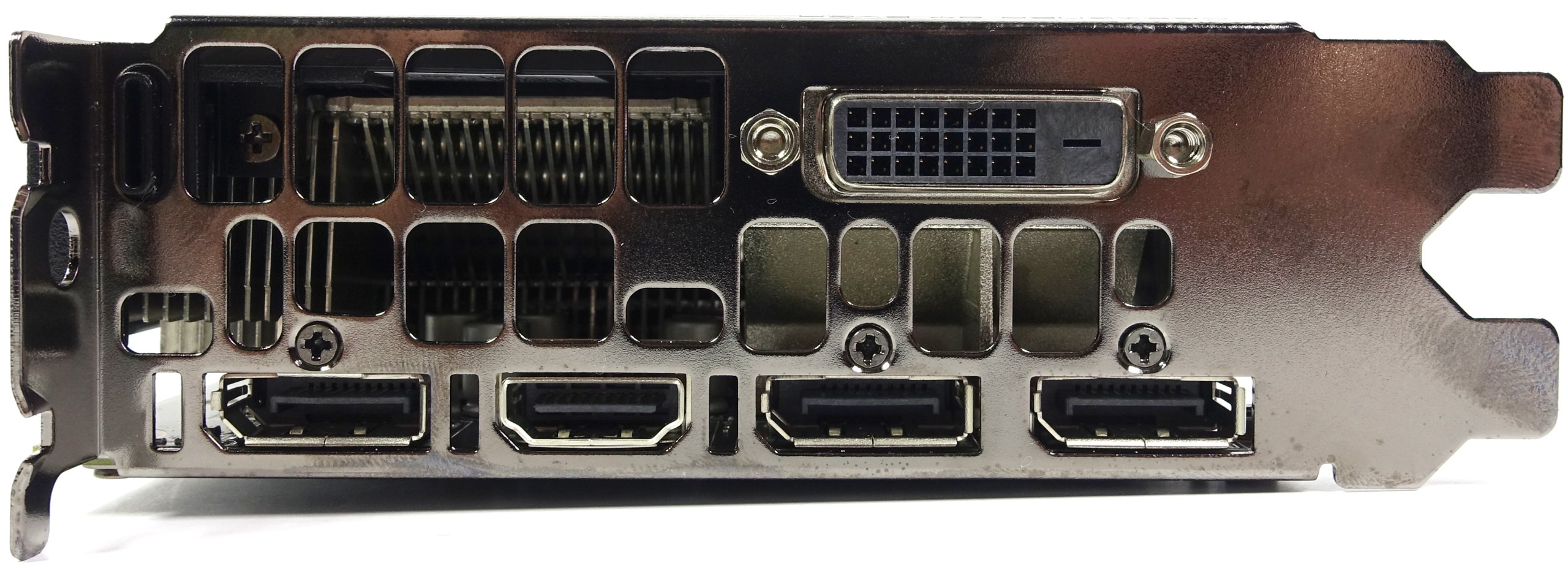
The slot aperture carries the usual five outputs, a maximum of four of which can be used together as part of a multi-monitor setup. In addition to the dual-link DVI-D (an analog signal is not looped through), there is an HDMI 2.0 output and three DisplayPort 1.4 ports on the back.
Board and assembly
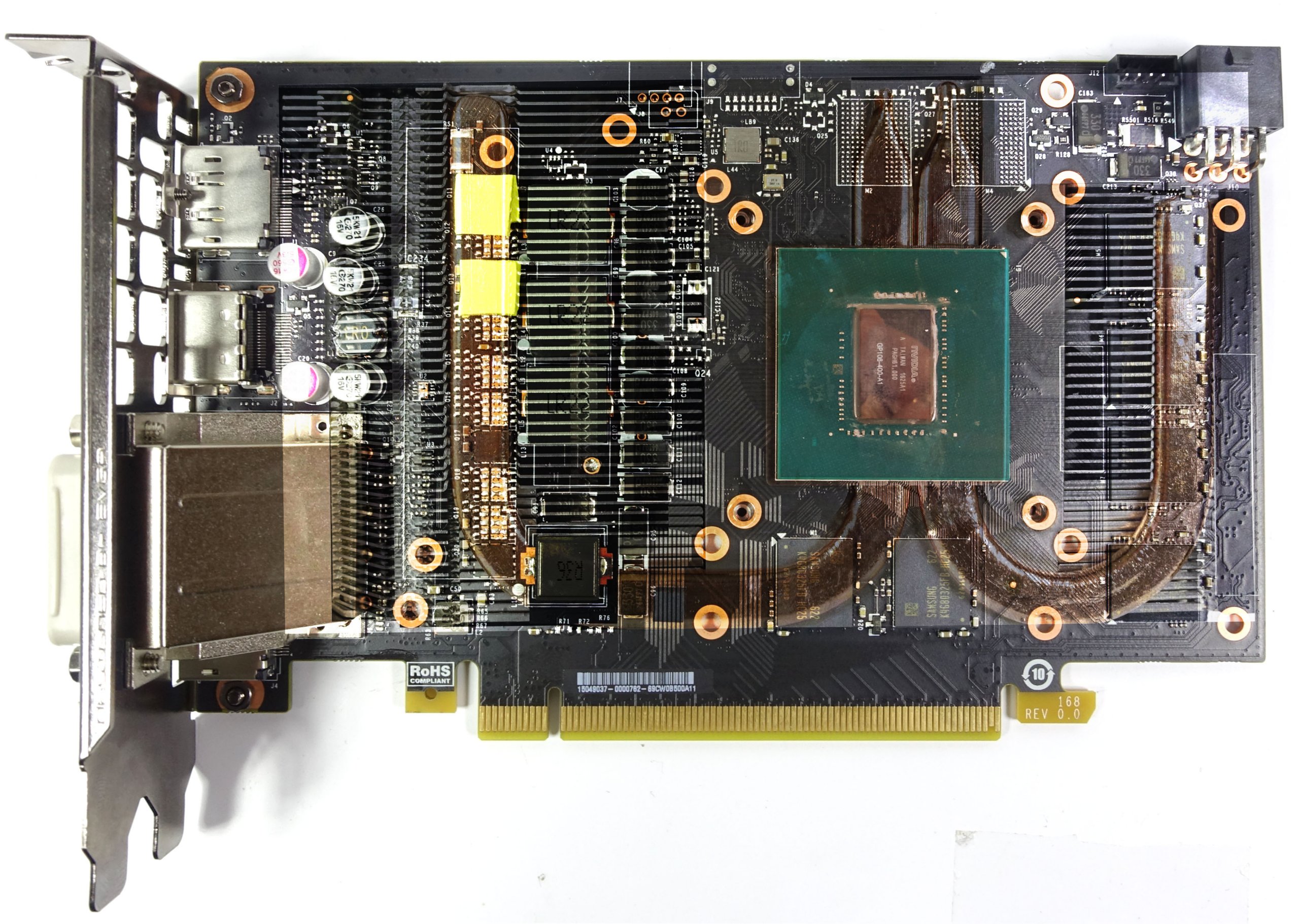
Let's take a closer look at the board, which is similar to the reference design, but differs in details. While the Nvidia board is manufactured in China, EVGA is the so-called Fabless supplier based on a Taiwanese supplier.
First, as with Nvidia's card, we see the four phases in total, three of which are allocated to the GPU and one to memory. Two of the three GPU phases are fed from the PCIe port, the third and the memory phase from the motherboard slot.
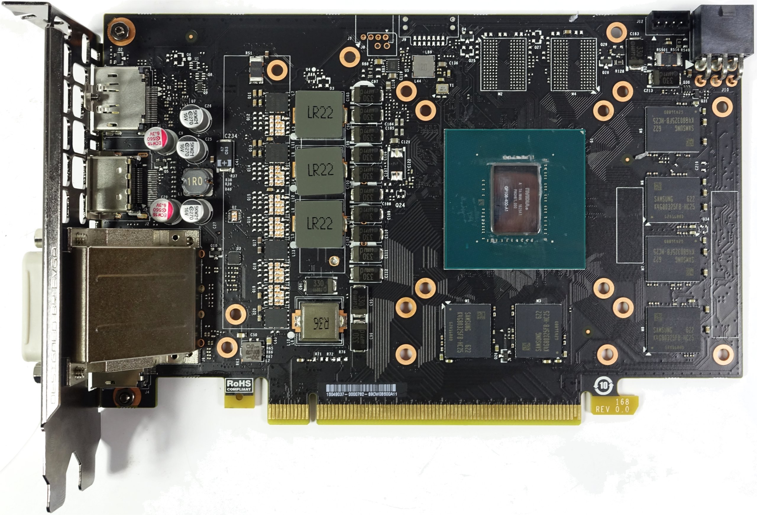
The motherboard would also offer the theoretical possibility to work with three phases and a maximum of six converter hoists via doubling for the GPU and a phase with a maximum of two converter hoists via Doubling for the memory, but the minimum assembly with only one As with the reference system, the converter pull per phase is designed for cost savings.
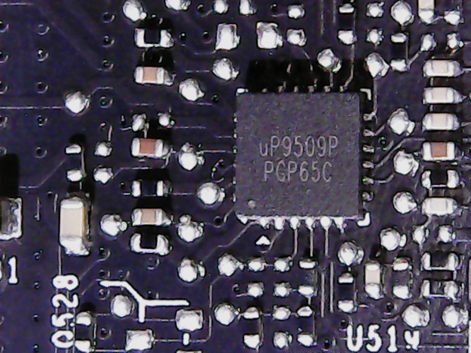
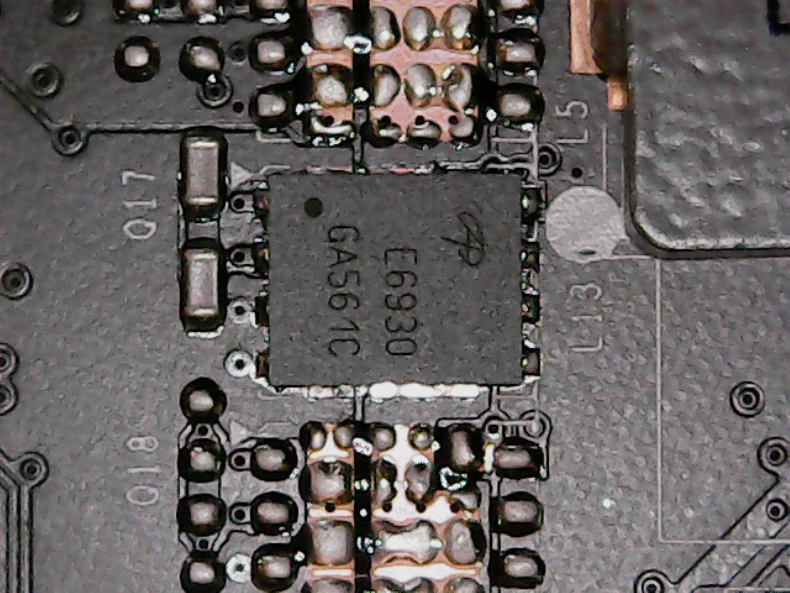
The three GPU phases are controlled by uPI Semiconductor Corp. via an uP9505P, each of which is realized with a higher-integrated dual-N-channel MOSFET E6930, which uses the gate driver, high- and low-side MOSFET, and the Schottky diode in a single Package united.
Cost and space savings here too, but the concentration of all components in a package also offers a significant disadvantage. This is because a thermal hotspot is created, which is also concentrated, because two of the MOSFETS are quite close together. Since the board is designed for doubling, one of the MOSFETS could have been placed on the empty position of the second converter train, which would have relaxed the situation somewhat. But more on that.
 |
 |
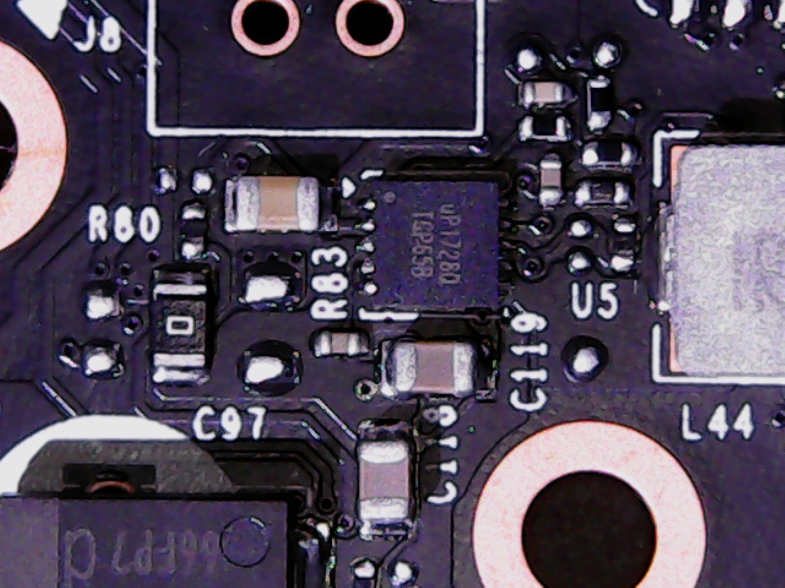
Below the GPU, two more capacitors are soldered to intercept and smooth voltage peaks – exactly the same principle as Nvidia's Refrenz. A small uP1728 from uPI Semiconductor Corp. is used to power the storage.
 |
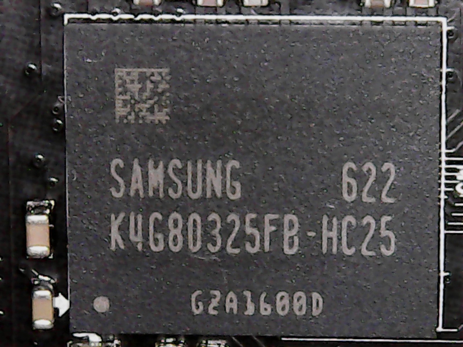 |
We note that only six of the eight existing memory fields are modules on this map. These are Samsung modules of the type K4G80325FB-HC25, each with a capacity of eight gigabit (32x 256 MBit) and can be operated with voltages between 1,305 and 1,597 volts, depending on the required clock. In total, this results in a total memory of six gigabytes.
Clock rates, voltages and power consumption
Of course, the course of boost clock and adjacent GPU core voltage as well as the connection between clock frequency and voltage are also interesting, whereby the clock curve breaks down a bit during gaming and when the card is fully warmed up.
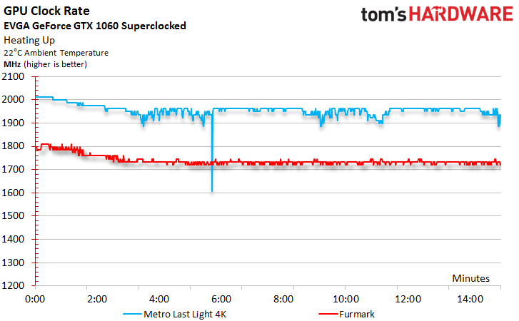
While the initial 2012 MHz boost clock falls on average after heating and under load to an acceptable 1949 to 1962 MHz (frequent fluctuations up and down included), the measured voltage values are quite similar: 1.062 volts on average for the warmed-up card reaches 0.975 volts, although it also varies between 1.025 and 0.9 volts.
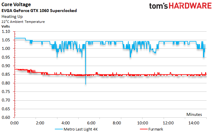
The reason is the intervention of Boost 3.0 and the rather low-set Power Target, which limits the power consumption to 120 watts and just above. These voltage curves and the flowing currents result in the already mentioned power consumption, which we can measure very well with our exact equipment at all connections.
As with the Gainward sister, the lowest GPU clock speed for idle measurement is approx. 253 MHz. The measured power consumption values are roughly at the level of the reference card, which is not surprising with such a low power target.
We worked with a variable low-pass filter for the measurements, so that we only mention possible, very short load peaks on the margins (greyed out bar), because they are hardly relevant in practice and have also irritated many readers. Nevertheless, the value determined here is quite high, which also suggests a not so optimal primary-side smoothing in front of the voltage converters.
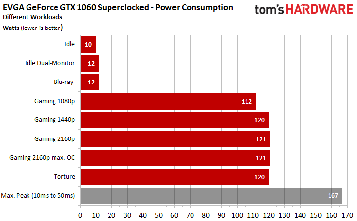
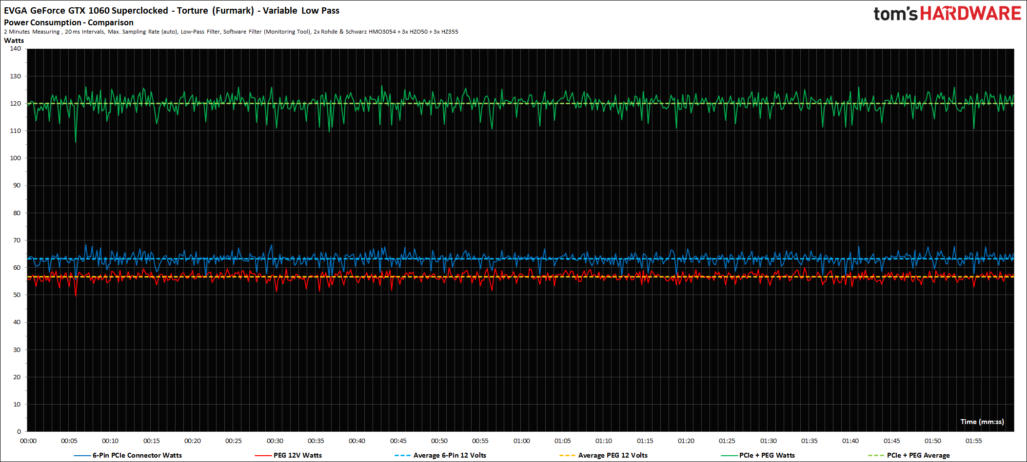
It is also the low Power Target that cuts the voltages during the stress test Boost 3.0 to such an extent that the power consumption is even slightly lower than in gaming, if you start the worst case there.
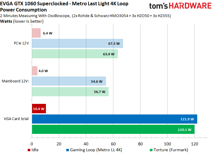
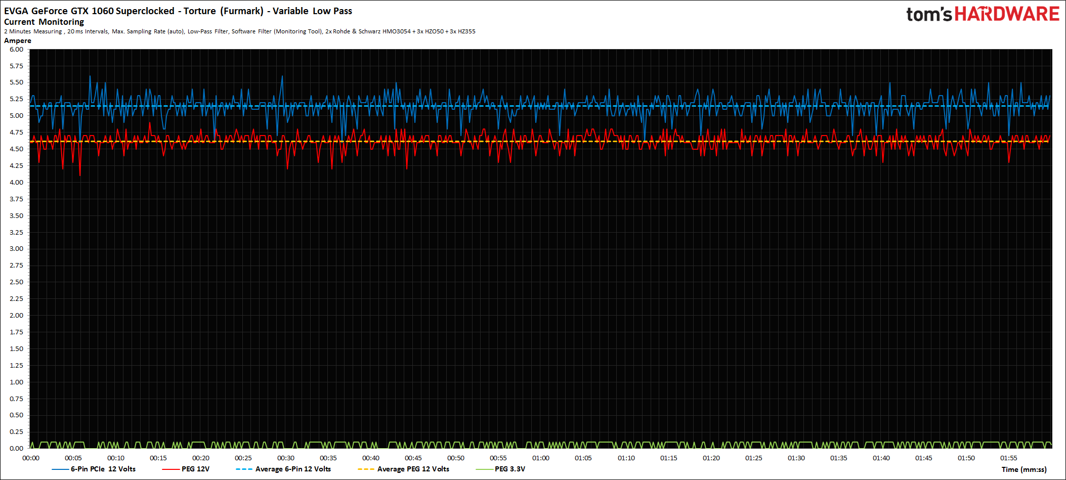
Loading of the power supply connections
Now we look at the division of the loads at maximum gaming load and the stress test: Since the 3.3V motherboard connection is not used at all, we have dispensed with this voltage rail in the diagrams.
The division of the four converter trains between the respective supply connections is completely uncritical, but also leaves no greater room for overclocking tests in accordance with the standards – but these are anyway provided by the BIOS (Power Target and voltage specification) slowed down:
Here's another clickable diagram with the respective history curves for gaming and stress testing:
 |
 |
Since the standards (PCI SIG) refer only to the flowing currents, we now look at the following diagrams, because the power consumption is only half the rent. With well under five amperes on the motherboard slot, however, you are absolutely on the safe side (PCI-SIG standard: max. 5.5 ampere):
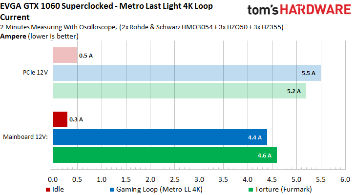
Of course, there are still clear large screens for the measured currents:
 |
 |
Cooling system, temperatures and a simple modification
Let's move on to the cooler and its conception, which has given us some headaches in the following. But the problem is easy to improve in just a few simple steps. Since EVGA expressly allows the removal of the cooler and does not threaten to lose warranty, we can describe our mod in detail in the following and above all encourage it to replicate – because it is worth it as long as EVGA does not improve itself.
If you remove the cooler, which is fixed with only four screws above the base, then you will see two wide-pressed 8 mm heatpipes, which are supposed to direct the heat absorbed by the copper heat sink directly to the slats at both cooler ends. The composite matrial used should handle both curvature and orientation reasonably efficiently.
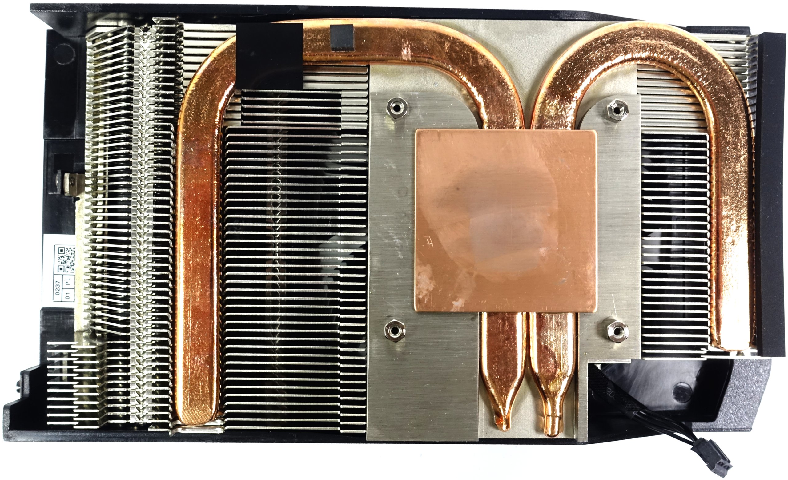
What we are already seeing, however, is the fact that neither the four dual-channel MOSFETs of the voltage converters nor the memory modules are actively cooled. This is where we will start right now and make a big difference with little effort.
The 9 cm fan used relies on conventional rotor blades, which are also quite steeply set to generate more pressure. Unfortunately, the heatpipes cover up some relevant areas (e.g. above the voltage converters) so that little of the air supplied arrives on the top of the board.
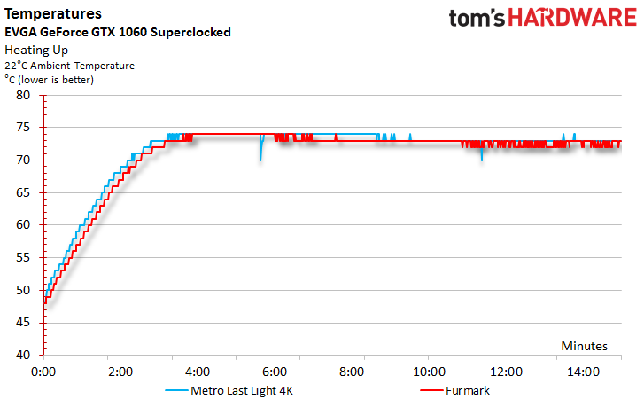
With the 73 to 74°C gaming loop (closed casing maximum 78°C), the cooler doesn't even do its service badly with regard to the GPU. The stress test shows a very similar picture, with the increase slightly flatter due to the lower clock and slightly lower power consumption. However, the final temperatures are almost identical.
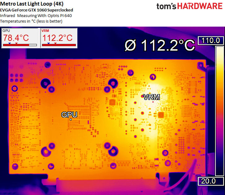
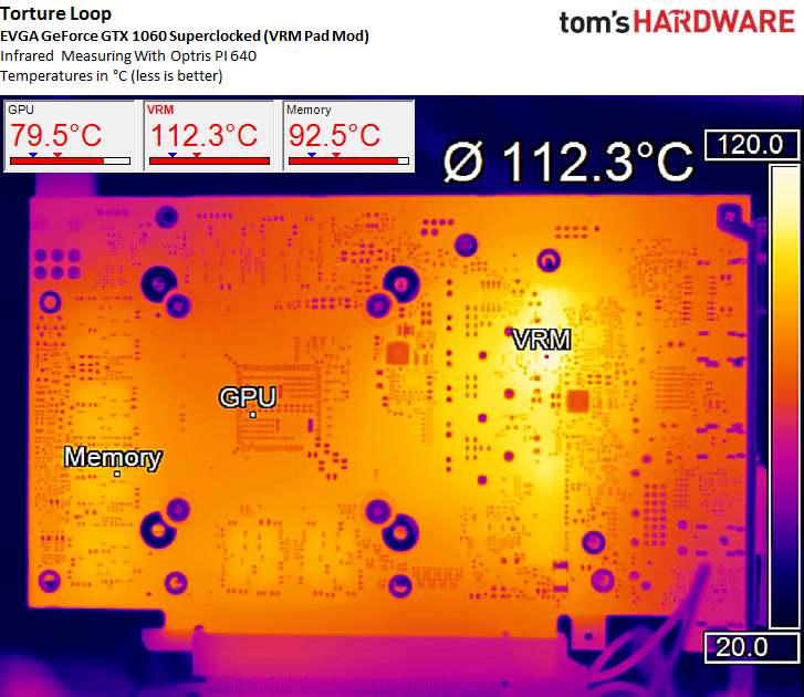
In the infrared measurement of the board, however, we see that the lack of active cooling of the voltage converters can take revenge. Already in the open setup you can reach 112°C in the gaming loop and in the stress test even above 119°C at the concentrated hotspot (see above). This would not even be critical for the installed MOSFETs as such, because they would still be within the specs up to 150°C. However, the waste heat travels through the copper-containing multi-layer board and spreads over a large area.
The p.r.a. p.r.o. (visible to the right of the VRM label as a pale rectangle) is located on the back side of the VRM label. 105°C also still in the possible frame, which would only come to an end at 150°C by inserting the OTP with a shut-down. It is already becoming more critical for the caps, whose pierced connecting wires act like small antennas and effectively direct the waste heat to the inside. With well over 100°C (stress test up to 112°C) a problem could arise here in the long run.
After all, we must not hide the fact that all these measurements were made in the air-conditioning area at only 22°C. In midsummer, smaller PC enclosures can easily be 40°C or more, which could push the above individual values even higher.
 |
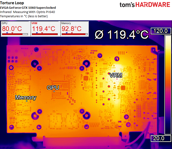 |
Nevertheless, the fact that the board below the socket is hotter than the values measured internally by the GPU diode shows us that the GPU here has to cool the hot board through the chip, which is really quite pointless. But this is easy to remedy and EVGA is obviously thinking about a change.
A mod for safety
The fact that the one heatpipe completely obscures the MOSFETs is now easy to take advantage of: For the sake of simplicity, we only reduce the large hotspot of the two upper GPU converter hoist strains with two superimposed thermal guide pads to reduce the bridge about two and a half millimetres difference. Of course, as an end user, you would want to equip all four MOSFETs in this way and thus achieve an even better result than we can:
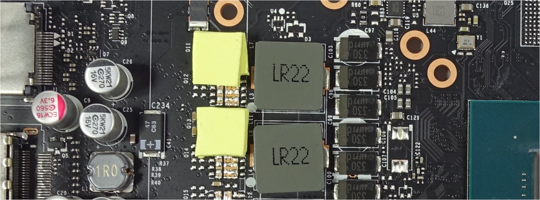
The following super projection clearly shows the position of the heatpipes, the components and our small aids in terms of cooling:
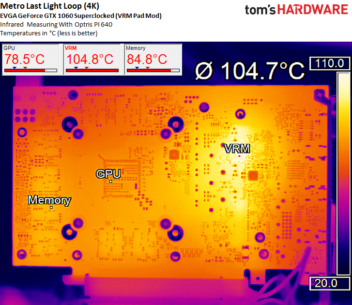
A new measurement with the infrared camera leaves us astonished: Minimal use of material, extremely large effect! With seven to eight Kelvin for only two of the four MOSFETs, we now come into a much calmer way to sleep in terms of long-term stability and the seam in smaller, not so optimally ventilated housings.
 |
 |
Noise
Hysteresis is not an issue for many manufacturers. EVGA also has a good grip on the principle as such, because at least after our BIOS update, the semi-passive mode also worked without annoying on-off-on loops. The threshold value for switching on the fan is approx. 65°C, but does not take into account the currently retrieved performance of the GPU.
However, we don't like the maximum 1000 rpm, because purely acoustically more could have been possible without torturing the ears. So you could easily lower the GPU temperatures by four to five Kelvin if you get more air with your own fan curve (important for ITX projects). The boost time would certainly be happy.
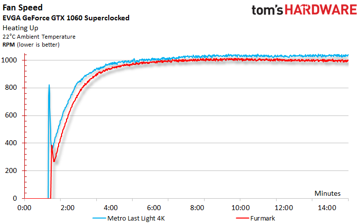
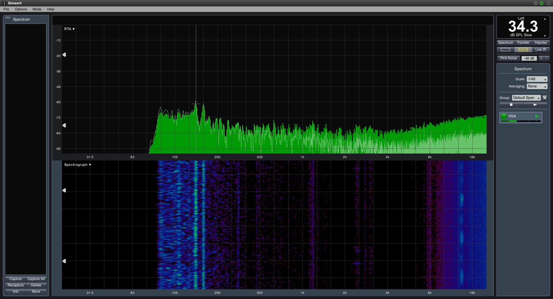
Due to the semi-passive mode, the noise in the idle is not measurable anyway, so we have completely dispensed with this one measurement. The noise of 34.3 db(A) under load, on the other hand, is already a real announcement and in the end results mainly from the very moderate fan curve. But even at 1300 rpm, one would still stay below the 36 dB (A) limit, which seems much more appropriate to us. EvGA probably just wanted too much here.
Technical data and interim conclusion
Let's take a look at the technical data and individual details of the graphics card:
- 1 - Einführung und Übersicht
- 2 - EVGA GeForce GTX 1060 Superclocked
- 3 - Gainward GeForce GTX 1060 Phoenix GS
- 4 - Gigabyte GeForce GTX 1060 G1 Gaming
- 5 - inno3D GeForce GTX 1060 Gaming OC
- 6 - MSI GeForce GTX 1060 Gaming X 3G
- 7 - MSI GeForce GTX 1060 Gaming X 6G
- 8 - Nvidia GeForce GTX 1060 Founders Edition
- 9 - Palit GeForce GTX 1060 SuperJetstream
- 10 - [Neu] PNY GeForce GTX 1060 XLR8 OC Gaming
- 11 - Vergleich der Gaming-Performance
- 12 - Vergleich vom Temperatur, Lautstärke und Leistungsaufnahme
- 13 - Vergleichende Zusammenfassung und Fazit


Kommentieren