


Teardown: PCB layout and components
Let’s start with the circuit board first. NVVDD is still the most important voltage and so this results in a voltage converter design with a total of 9 true phases (instead of 6 on the FE and most MSRP boards) and the resulting 9 control loops for NVVDD alone. Thus, you do not save quite as much compared to the RTX 4070 Ti, but this is completely acceptable in view of the significantly lower TDP. 10 phases, as in the case of Asus’ cards, can definitely be done, but it actually doesn’t bring anything more besides a marketing highlight.
From a technical point of view, this is nonsense, because you would have to change the balancing a bit. We can see the last free space above the PCIe slot on the picture of the board and thus also that this tenth phase should have been connected to the slot. However, there are already plenty of 4 amps at 215 watts (of a maximum of 5.5 allowed), so that another phase would quickly reach the limits of the PCI SIG if the 240 watts TBP were really utilized. Then rather as shown.
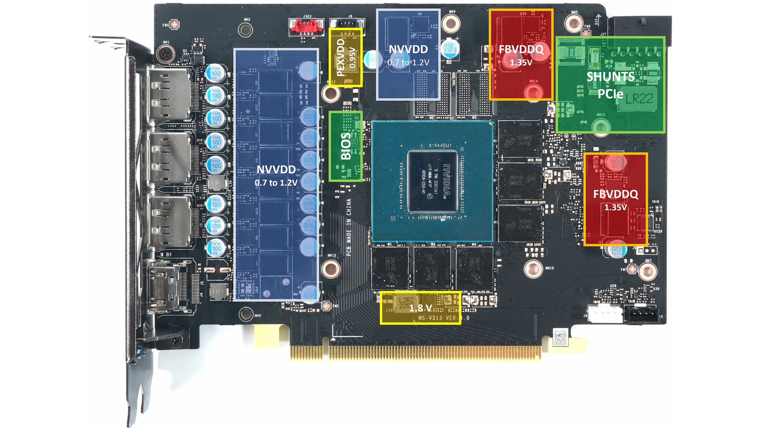
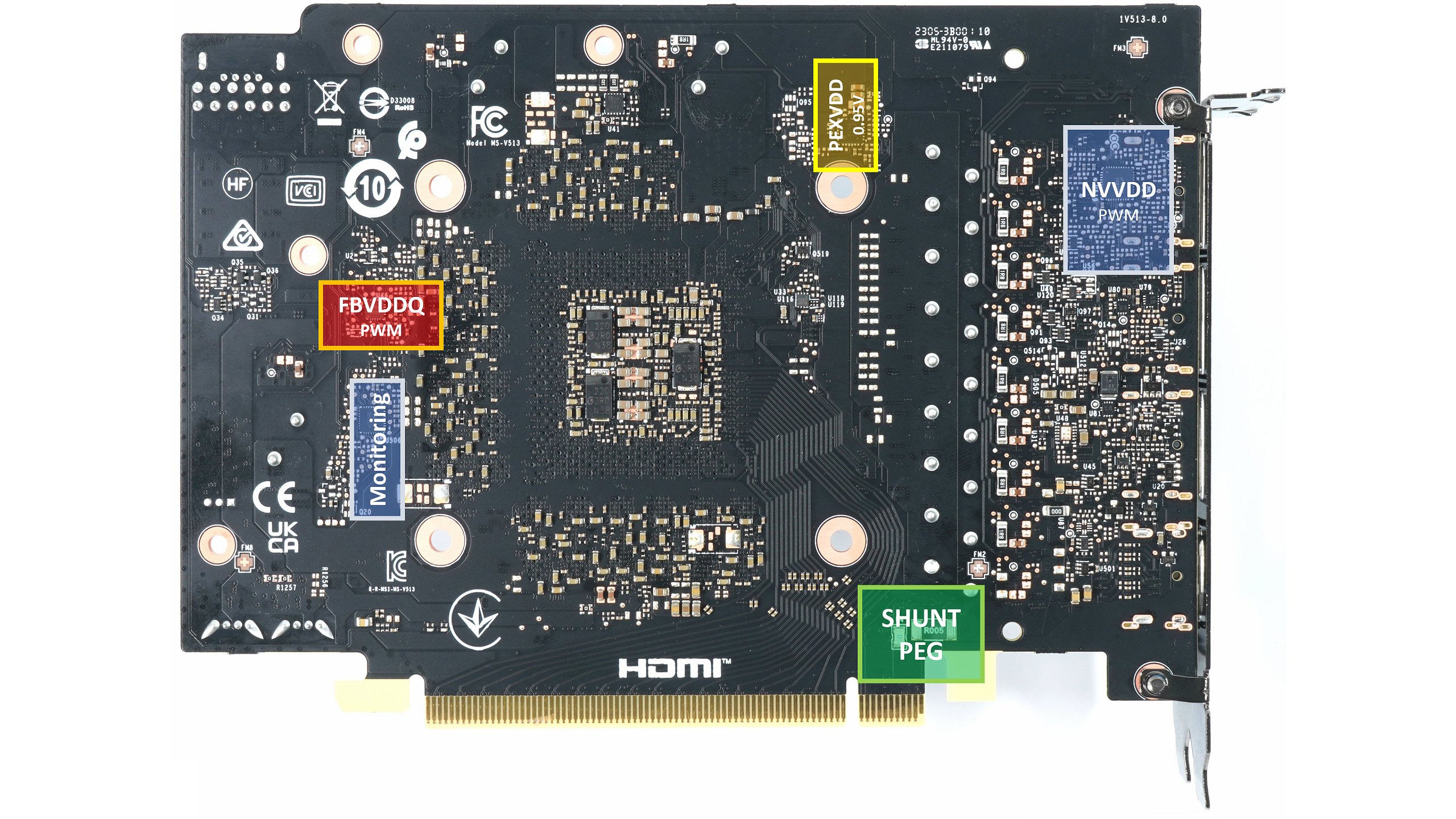
This doesn’t look quite as lean as it did with the FE, which is reassuring. One also uses separate PWM controllers for NVVDD (GPU core) and FBVDDQ (memory), because the top models among the PWM controllers are unfortunately much too expensive. And that’s why the good and well-known uP9512R from UPI Semi has to do it again, which can also generate phases with a trick and is significantly cheaper than the models from Monolith, which, however, is completely sufficient. A second PWM controller in the form of the small uP9529 then controls the two phases for the memory. By the way, both controllers are located on the back of the board. Directly in between is a uPI uS5650Q for monitoring the four 12V rails (3x Aux and 1x PEG).
All DrMOS used, including those for the memory, are rather cheap products from Alpha & Omega, which we already know from the MSI RTX 4070 Ti Suprim X. The 55 A peak current AOZ5311NQI BLN30 used in all control loops for NVVDD and FBVDDQ (memory) integrates a MOSFET driver, high-side MOSFET and low-side MOSFET in a single package. This chip is specifically designed for high current applications such as DC-DC buck power conversion applications. This integrated solution reduces the space required on the PCB compared to a solution with discrete components. The coils used for NVVDD and the memory have an inductance of 220 nH, and the capacitors are in cup form, which is cheaper.
The 12V rails on the 12+4 12VHPWR connector are combined into a single rail directly after the socket, another is connected to the PEG, and is only slightly used for NVVDD. The BIOS is in the usual place and the generation of the remaining extra-low voltages is also as usual. The GDDR6X memory chips are manufactured by Micron and bear the model number D8BZC, which is decoded to MT61K512M32KPA-21:U. They are specified for a clock frequency of 1313 MHz (21 Gbps GDDR6 effective). There are no more special features.

Teardown: The cooler
MSI relies on well-known fans, in this case even three. With the 9.5 cm rotor blades (opening 10 cm), the three identically aligned fans, each with 9 rotor blades, emit a concentrated airflow towards the radiator thanks to the circumferential ring, resulting in less turbulence and losses at the air intake of the radiator cover.
A total of 6 nickel-plated heatpipes made of copper composite material lead from the heatsink to the end of the extra-long cooler, a large part of which also protrudes over the very short PCB. This results in a welcome “draught”, as there is no PCB to slow down the airflow. Three of the heatpipes then also lead towards the slot bracket and back again. This is also where the VRM heatsink is located, which is much more stable compared to the MSI RTX 4070 Ventus and does its job more than just sovereign this time. The single NVVDD phase on the card’s upper side and the two voltage converters for the memory are also actively and validly cooled by adapted, additional cooling surfaces.
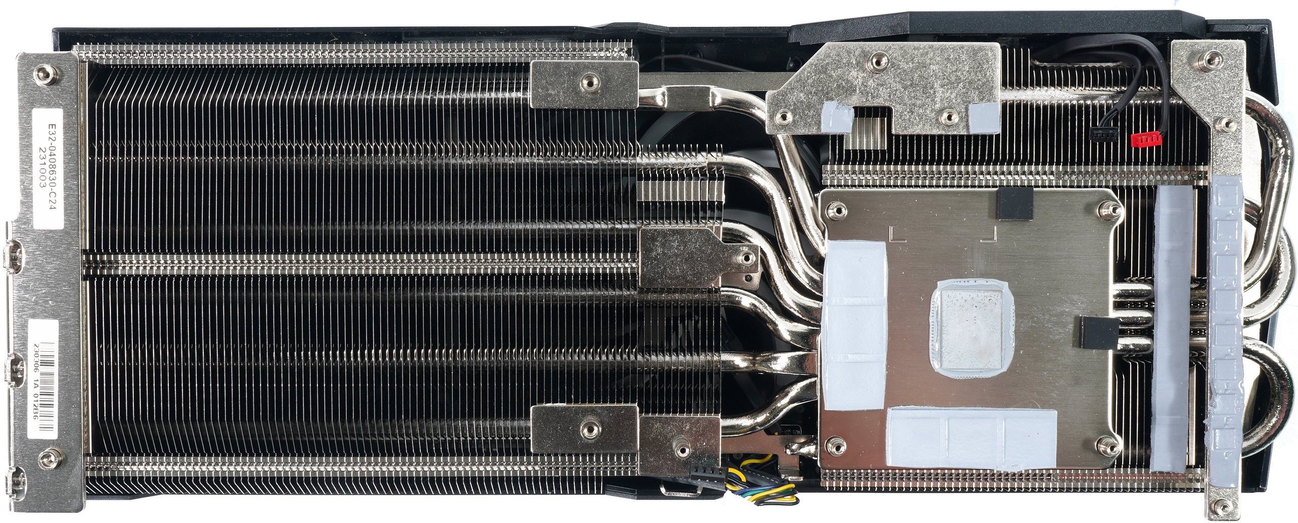
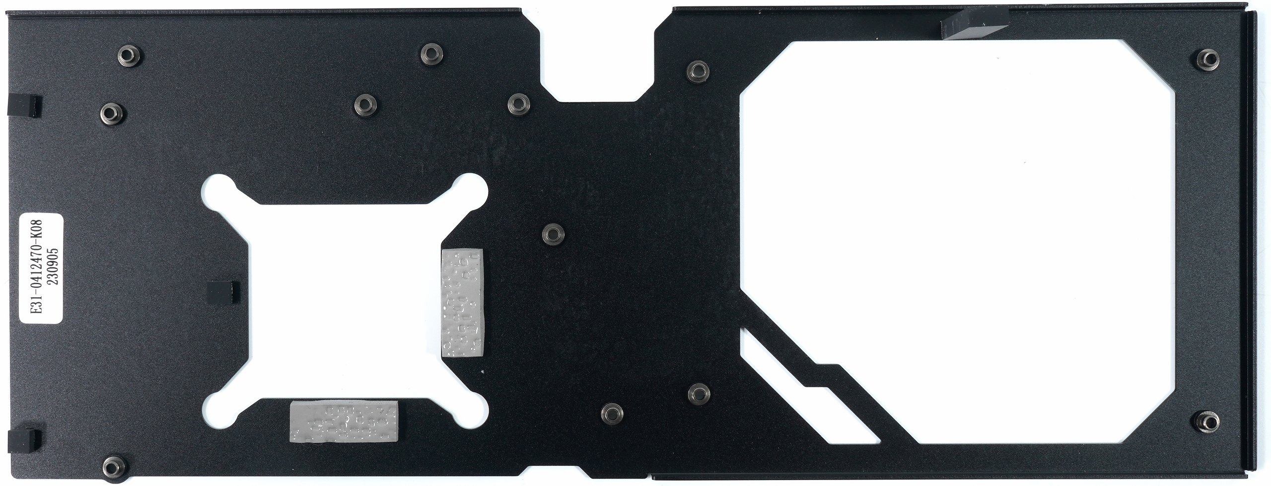
The pads used are ok, but not top shelf. So you’ll find some cost-down here, too. The metallic backplate is not only screwed to the PCB this time, but directly to the cooler with a lot of individual screws. This stabilizes the board and prevents it from bending during horizontal assembly. This also guarantees a consistently good contact pressure on the areas to be cooled. I already wrote something about the airflow, and we can still see the appropriate cutout for it here (right).

- 1 - Introduction, technical data and technology
- 2 - Test system and methods
- 3 - Teardown: PCB, components and cooler
- 4 - Gaming performance
- 5 - Details: Power consumption and load balancing
- 6 - Transients and PSU recommendation
- 7 - Colock rate, temperatures and thermal imaging
- 8 - Fan speed and noise level
- 9 - Summary and conclusion


70 Antworten
Kommentar
Lade neue Kommentare
Urgestein
1
Urgestein
Urgestein
1
1
Urgestein
1
Urgestein
Urgestein
Urgestein
Urgestein
Urgestein
1
Urgestein
Urgestein
Urgestein
Mitglied
Urgestein
Alle Kommentare lesen unter igor´sLAB Community →