


Board analysis and power supply
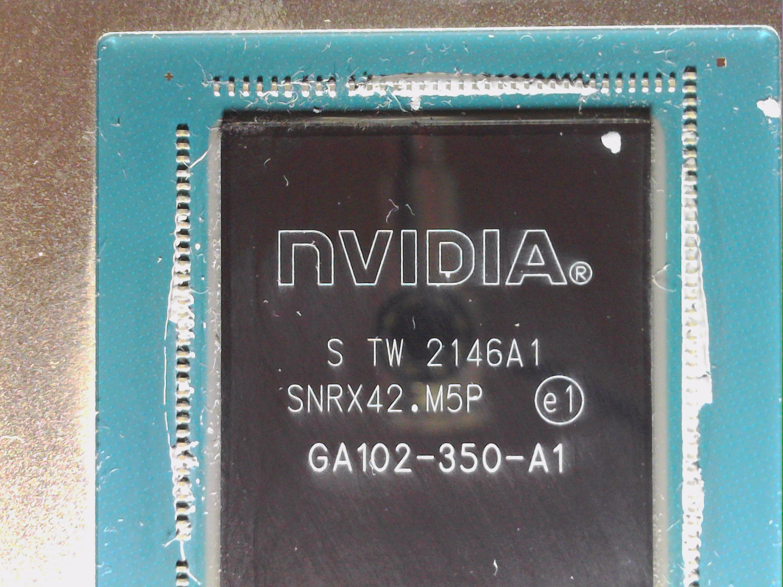
As usual, the 12-layer board relies on the backdrill method, which already shows why I called the GeForce RTX 3090 Ti a “playground” for the upcoming GeForce RTX 4090/4080. The type of power supply also differs from the GeForce RTX 3090 and does away with the previous dichotomy of the main power supply. NVVDD stands for the conventional core voltage, i.e. what we like to call GPU voltage, MSVDD is omitted again. A total of 24 voltage converters for the GPU alone also correspond to what NVIDIA has planned for the upcoming generation on the reference board (see schematic). If you would like to know more about this, you are welcome to read the relevant article beforehand.
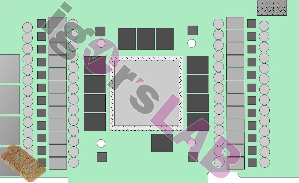
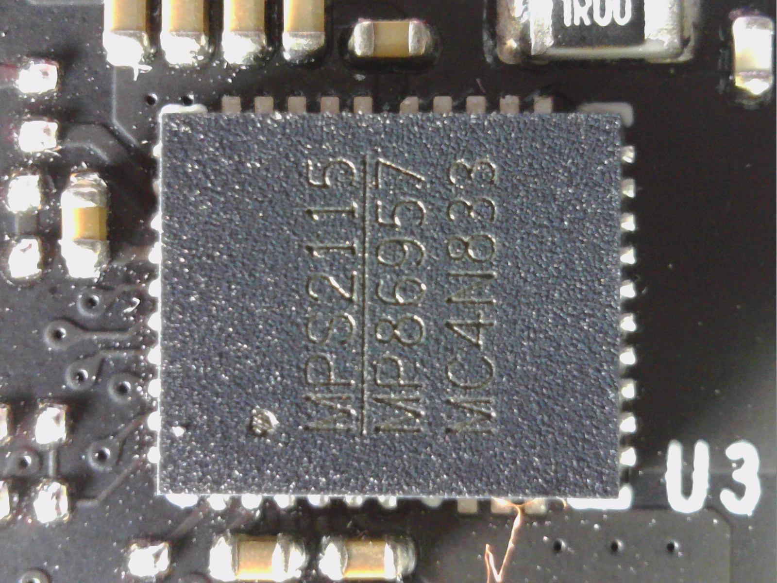
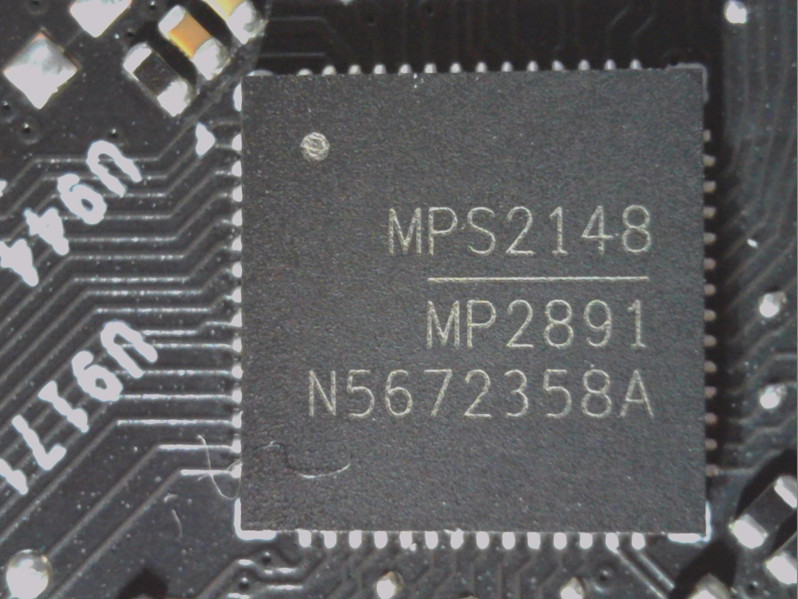
It should also be eight individual phases in the MSI GeForce RTX 3090 Ti SUPRIM X, but they are tripped to 24 and provided by a (unfortunately hardly documented) Monolith MP2891 on the back. This is a digital PWM controller with VID interface, compatible with NVIDIA’s Open VReg specification and various expansion functions. MSI relies on Monolith’s MPS2115/MP86957 for all 24 voltage converters that are controlled with it. These mighty components are supposed to keep the load peaks lower than some would fear.
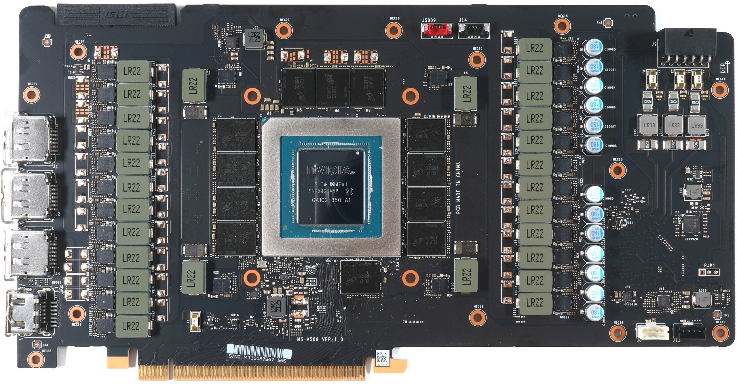
The installed MP86957 is a monolithic half-bridge with integrated power MOSFETs and gate drivers. It achieves quite high continuous output current over a very wide input supply range, making it a monolithic IC approach that can handle up to 70A per phase. The integration of drivers and MOSFETs results in high efficiency due to optimal dead time and reduction of parasitic inductance. It can operate at frequencies from 100 kHz to 3 MHz and uses a tri-state PWM signal via the appropriate controller. It also features Accu-SenseTM current sensing to monitor inductor current and temperature sensing to report junction temperature, making it a true Smart Power Stage (SPS).
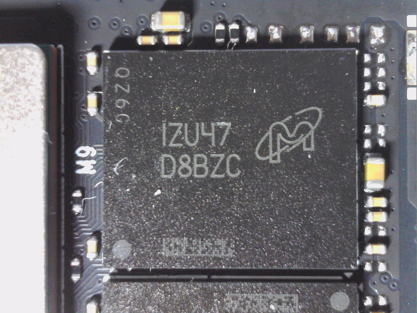
For the fast GDDR6X memory from MICRON (D8BZC) in the form of 12 modules with 2 GB memory capacity each, a total of four voltage converters are used (2 doubled phases), which are also controlled by the MP86957. All four voltage converters are also MP86957 from Monolith and the same 220 mH coils are used as in NVVDD for the GPU. The PLC of the PCI Express voltage PEXVDD and the 1.8 Volt converter are located on the front, the corresponding coils as well. There is also a 5V filter at the bottom right.
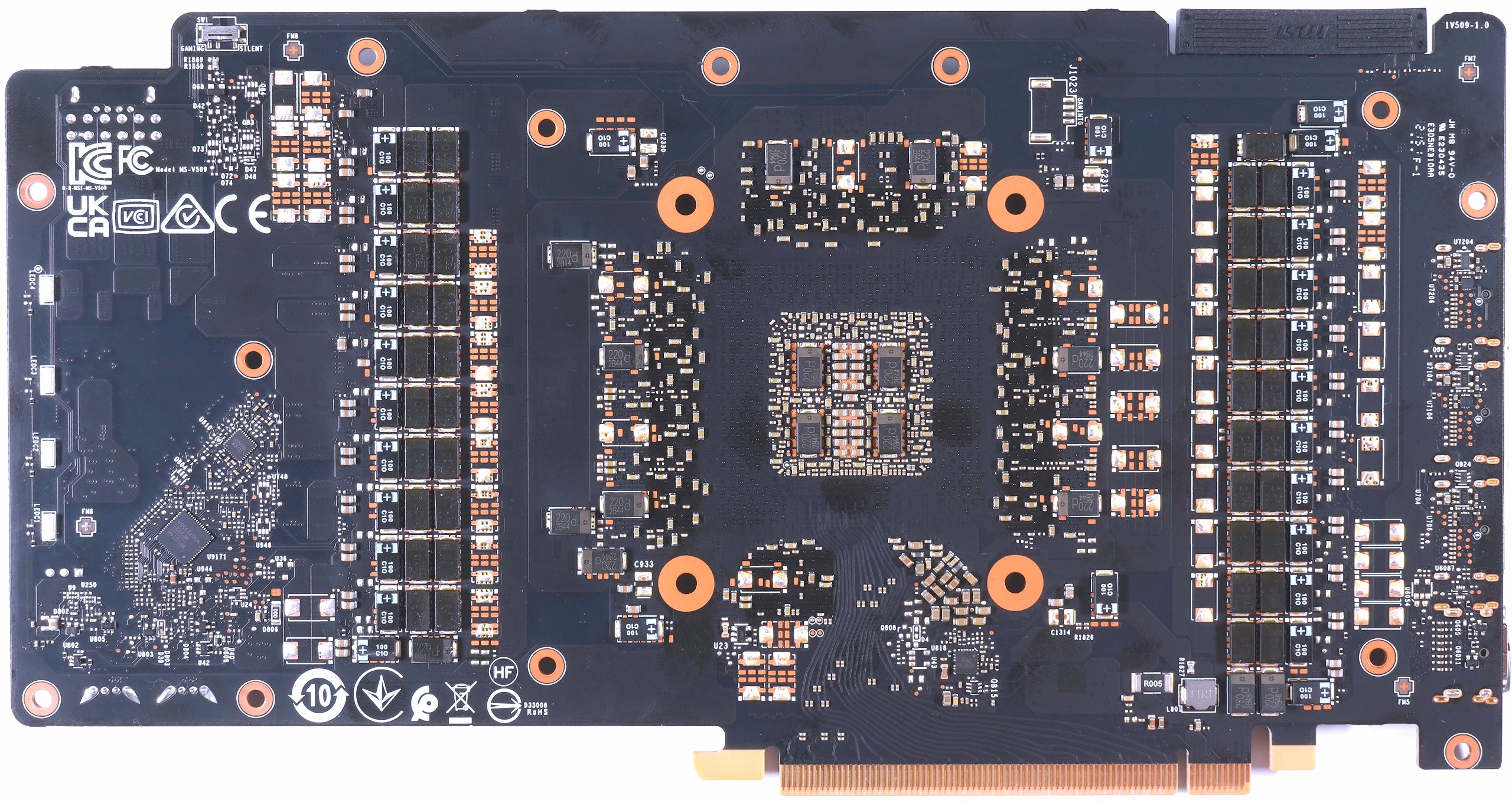
Interesting on the back is the use of polymer capacitors underneath the memory modules. According to internal information, these caps are used for stabilization. Obviously, one cap per module is used for the AD102, while the soldering areas under individual modules were not equipped here, for whatever reason.
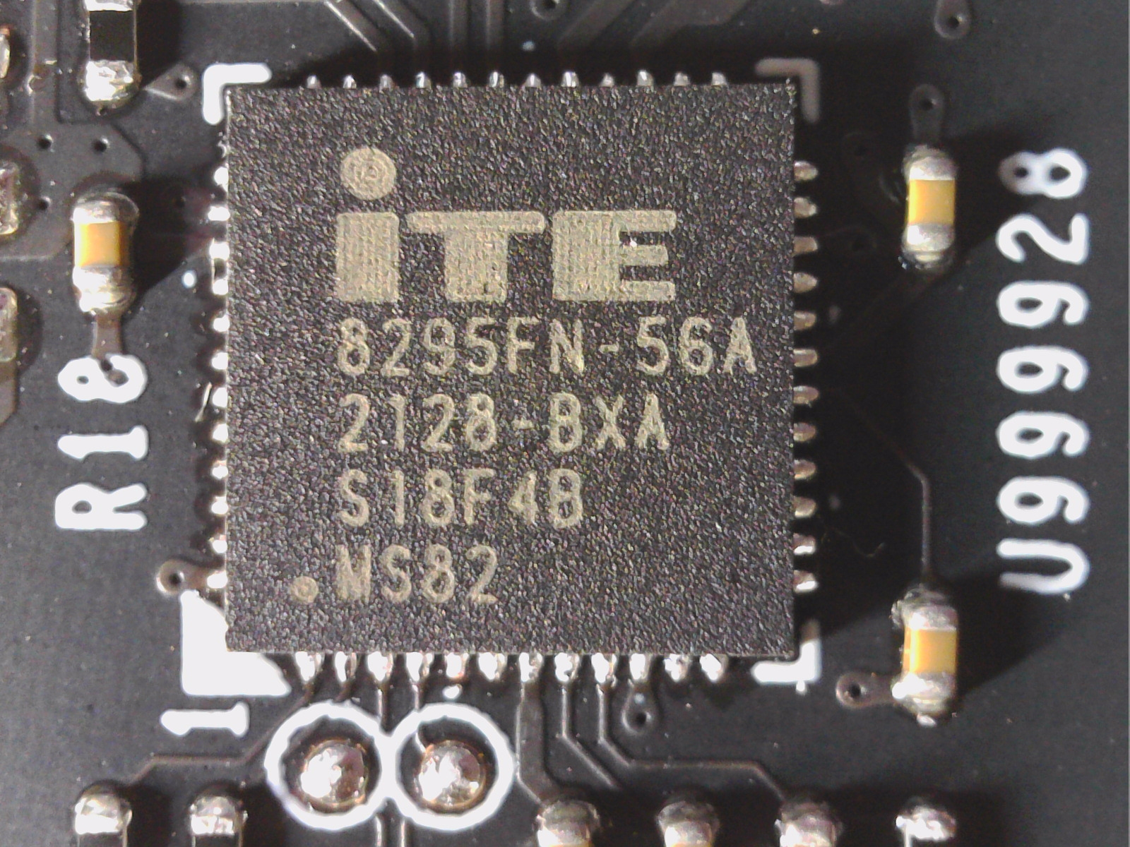
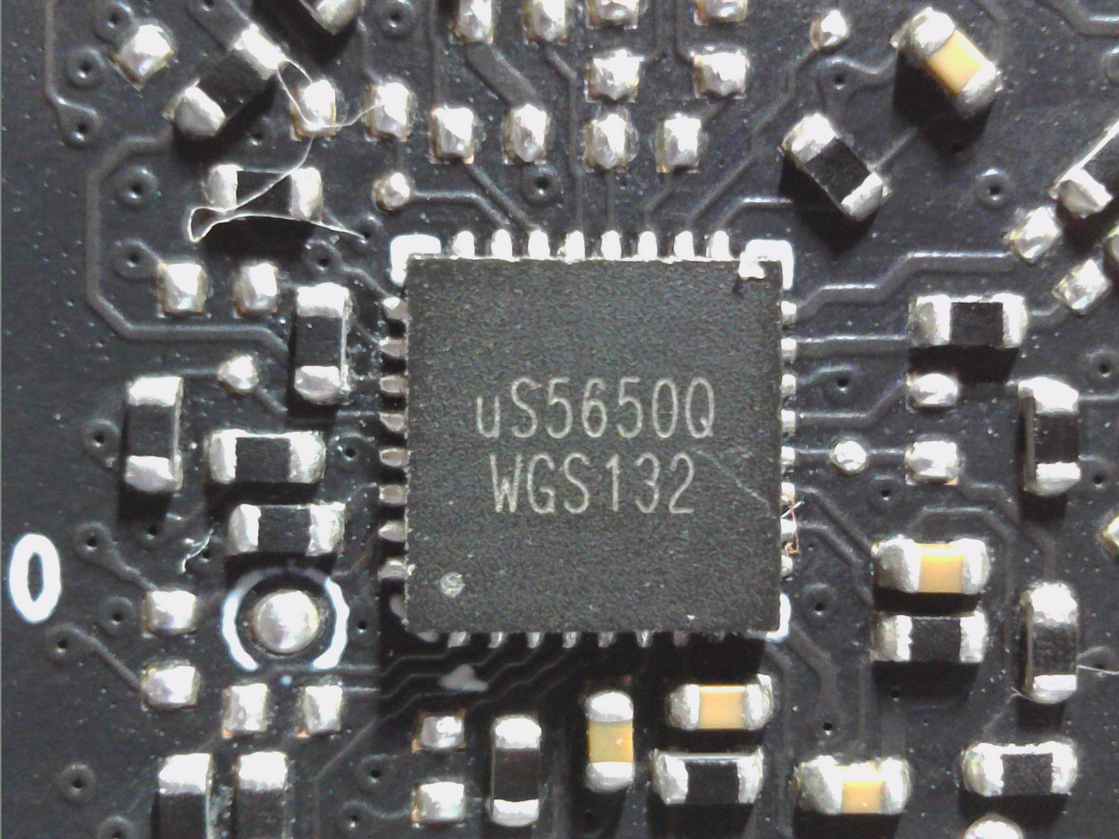
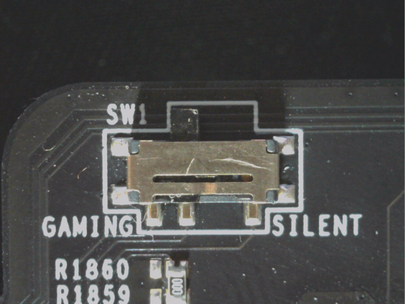
To smooth the three 12V rails and to reduce the load peaks in the area of the new 12+4 connector (2 rails of the socket each go together to one of the three rails), there is one RC element each consisting of a low impedance power resistor and a coil with 330 mH (front side) in front of which a shunt is placed. The voltage drop of the shunt is used to measure the flowing currents. A uS5650Q from UPI is used for this (back, next to the PWM controller). The DIP switch is for switching between gaming and silent mode, that’s about it. The following pictures show the mentioned components once again in detail:

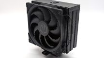
Cooler and disassembly
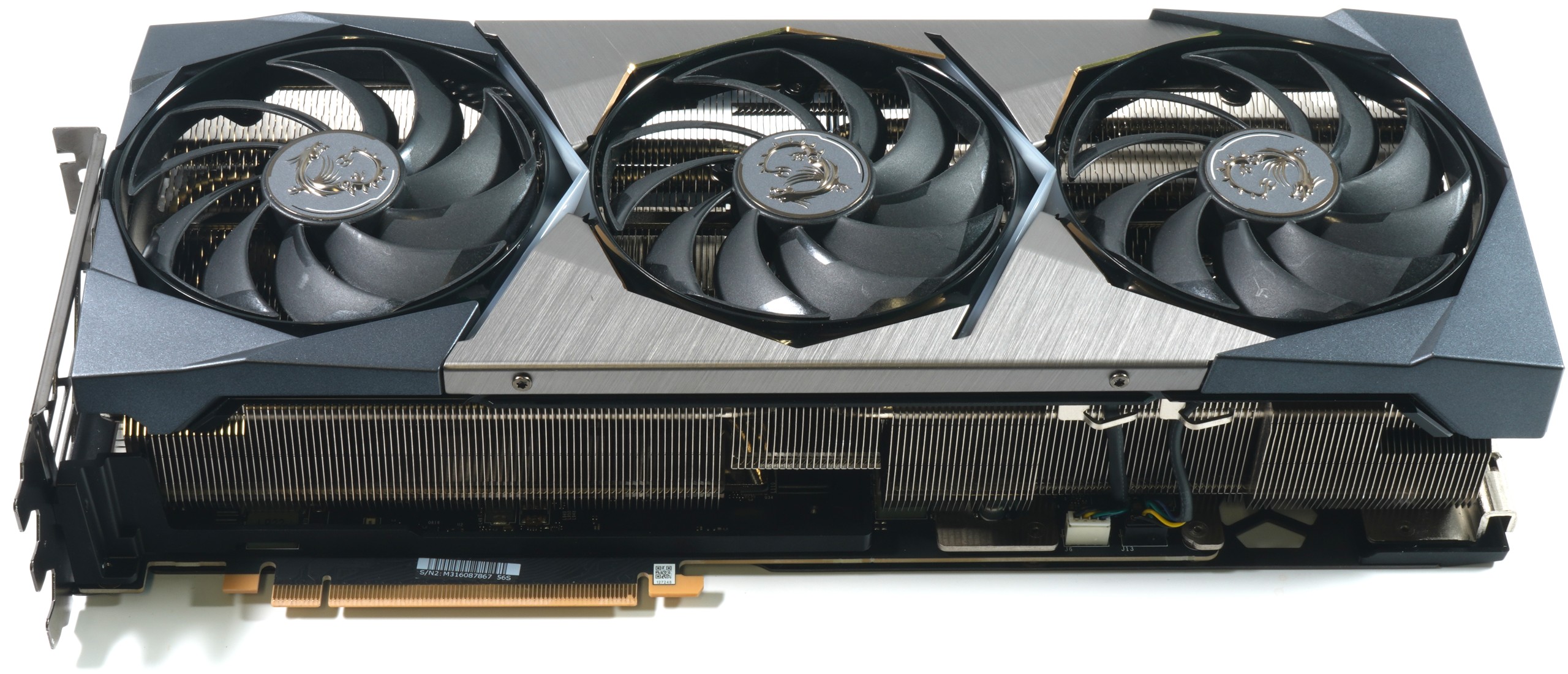
The front is characterized by three 10 cm fans with 10 rotor blades each, which are combined into 5 double blades each and act quite quietly. There are no more special features to observe from above and outside for the time being. The cooler cover is supported by the cooler and has no connection to the PCB or backplate.
Disassembly is therefore simple. After unscrewing the backplate, the screws for fixing it to the PCB and the GPU cross, the cooler can also be removed completely quite easily. You just have to disconnect the two fan cables and the RGB cords. The extremely thick, very soft pads on the memory modules and the VRM ensure that even possible manufacturing tolerances of the package of up to 0.5 mm in height can be easily compensated. MSI has accepted the criticism of the bleeding pads and relies on soft but crumbly pads that are very similar to those from Fujipoly and are not oily.
We see a total of eight (!) nickel-plated 6 mm heatpipes made of copper composite material, which were soldered to the back of the heatsink above the GPU. Two of the heat pipes (the two outer ones) are only effective in the GPU area, two of the six continuous heat pipes (the two inner ones) are also bent backwards. The memory is cooled by the heatsink via the thick, very good pads, the voltage converter heatsinks sit separately. The coils are only partially cooled here.
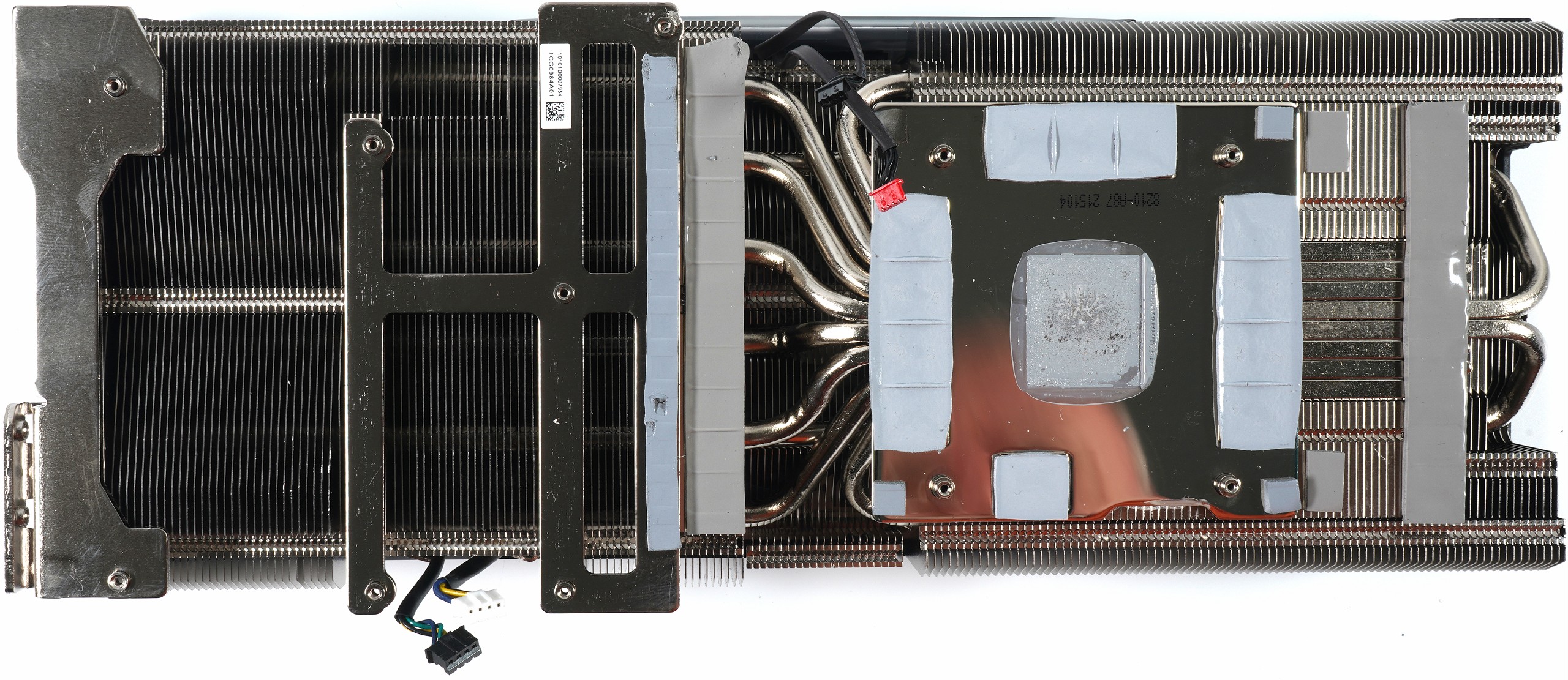
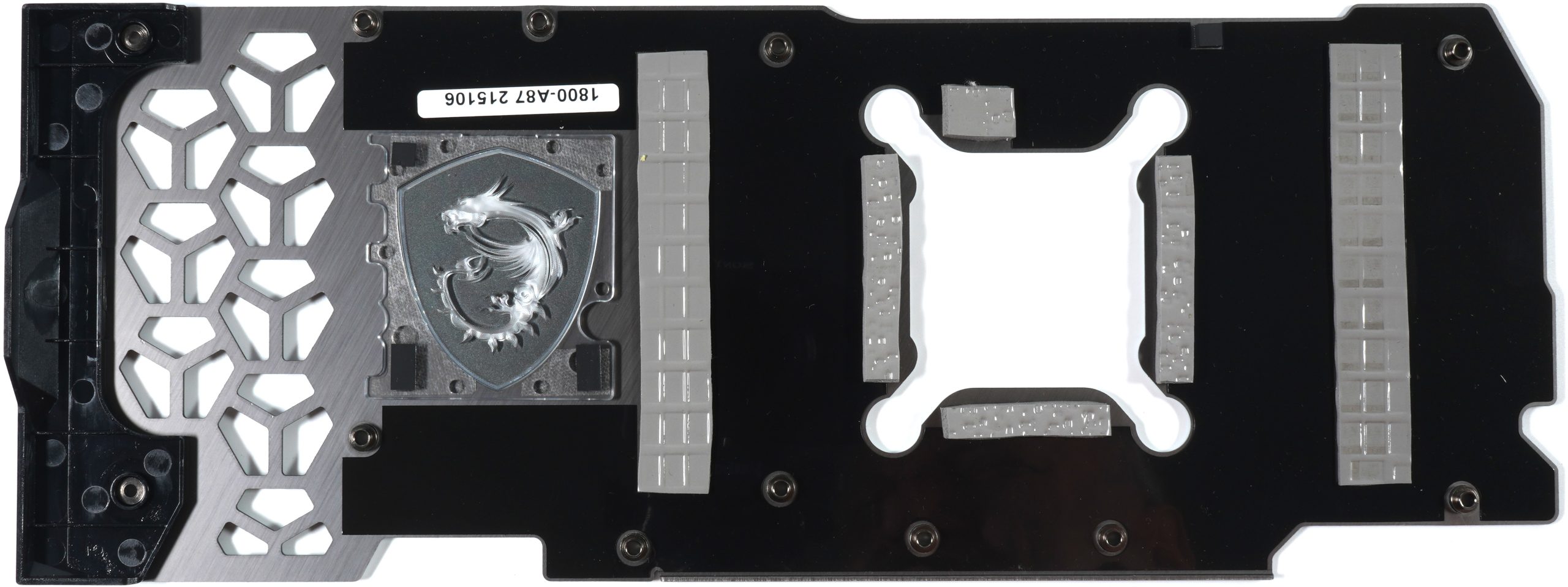
On the back, you’ll find a backplate made of light metal, which also fulfills its function in terms of cooling and doesn’t just serve to look good and stabilize the cooler assembly together with the PCB. The voltage converter areas, as well as the GDDR6X memory and its capacitors are cooled on the back.

- 1 - Introduction, Unboxing and Technical Data
- 2 - MSI's PSU, Test System and Test Methods
- 3 - Teardown, PCB Analysis, Components and Cooler
- 4 - Gaming Performance (Bars)
- 5 - Gaming Performance (Curves)
- 6 - Percentiles (Curves)
- 7 - Frame Times (Curves)
- 8 - Frame Times (Bars)
- 9 - Variances (Bars)
- 10 - Power Draw GPU in Detail (Each Game)
- 11 - Power Draw CPU in Detail (Each Game)
- 12 - Effiziency in Detail (Each Game)
- 13 - Power Consumption in Games and Applications (Average)
- 14 - Transients, PCIe Standard and PSU Recommendation
- 15 - Temperatures and Thermal Imager
- 16 - Fan Speed, Noise, Coil Whining
- 17 - Summary and Conclusion


52 Antworten
Kommentar
Lade neue Kommentare
Urgestein
Mitglied
1
Urgestein
Moderator
Veteran
Urgestein
Mitglied
Urgestein
Veteran
Urgestein
Urgestein
Veteran
Mitglied
Urgestein
Urgestein
Urgestein
Veteran
Mitglied
Alle Kommentare lesen unter igor´sLAB Community →