


Actually, everyone had already checked off the Ampere generation, but then came CES 2022 and Jensen with the GeForce RTX 3090 Ti. One can really argue about the sense or nonsense of this card in the full version of the GA102 and the high-energy implementation, but it exists and would like to be tested and evaluated. And while we are at it, this card already has a kind of special position in the transition to the next generation. It is in fact a card that NVIDIA launches completely without need, because the competitors already have to nibble at the GeForce RTX 3090. So what’s the point of such a monster, which first has to manage the balancing act between crowbar and added value?
I therefore took longer this time to analyze the technology and was also able to find many interesting parallels to what I had already written about with regard to the new Ada cards with the AD102. Yes, you can already see the first traces of the next generation and yes, the GeForce RTX 3090 Ti is also faster than the previous GeForce RTX 3090. And it is precisely the technical changes required for this, up to and including the rather unrestrained use of electrical energy, that I will be reporting on today. The benchmarks including all metrics are of course included for free, as usual. Plus a nice summary with averages across all 10 games in 3 screen resolutions. Oh, there are also various surprises, but more about that later.
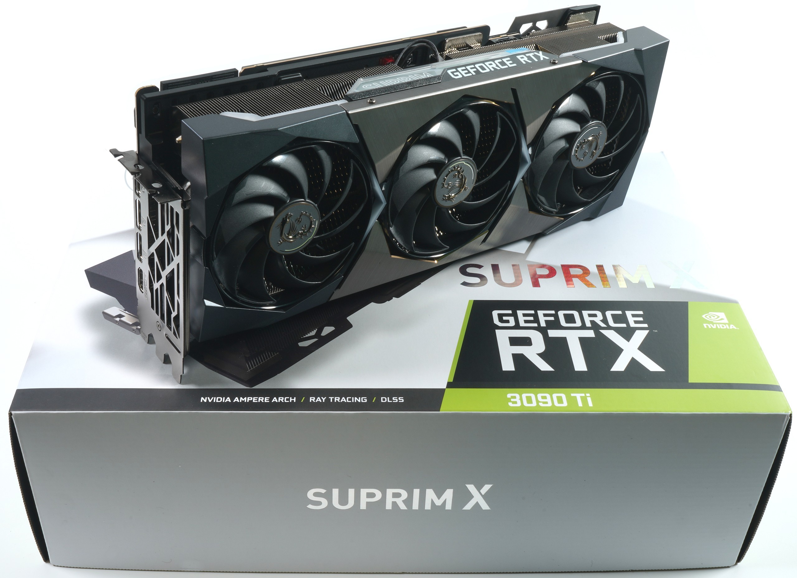
Since there is no Founders Edition of the GeForce RTX 3090 Ti available as a sample, I will rely on an MSI GeForce RTX 3090 Ti SUPRIM X for today’s test, which was kindly provided to me by MSI in advance. However, since it would be pointless to test this performance-enhanced card against reference models, I also put MSI’s so-called custom models against it for all of the cards represented in the test. For the NVIDIA cards, all the cards come from the Suprim (X) series, while for the AMD cards, I use the Gaming X models for lack of other versions. Thus, they are all factory overclocked cards in gaming mode and with a consistent manufacturer philosophy. Anything else would really be window dressing. Therefore, the test is also limited to 7 relevant cards.
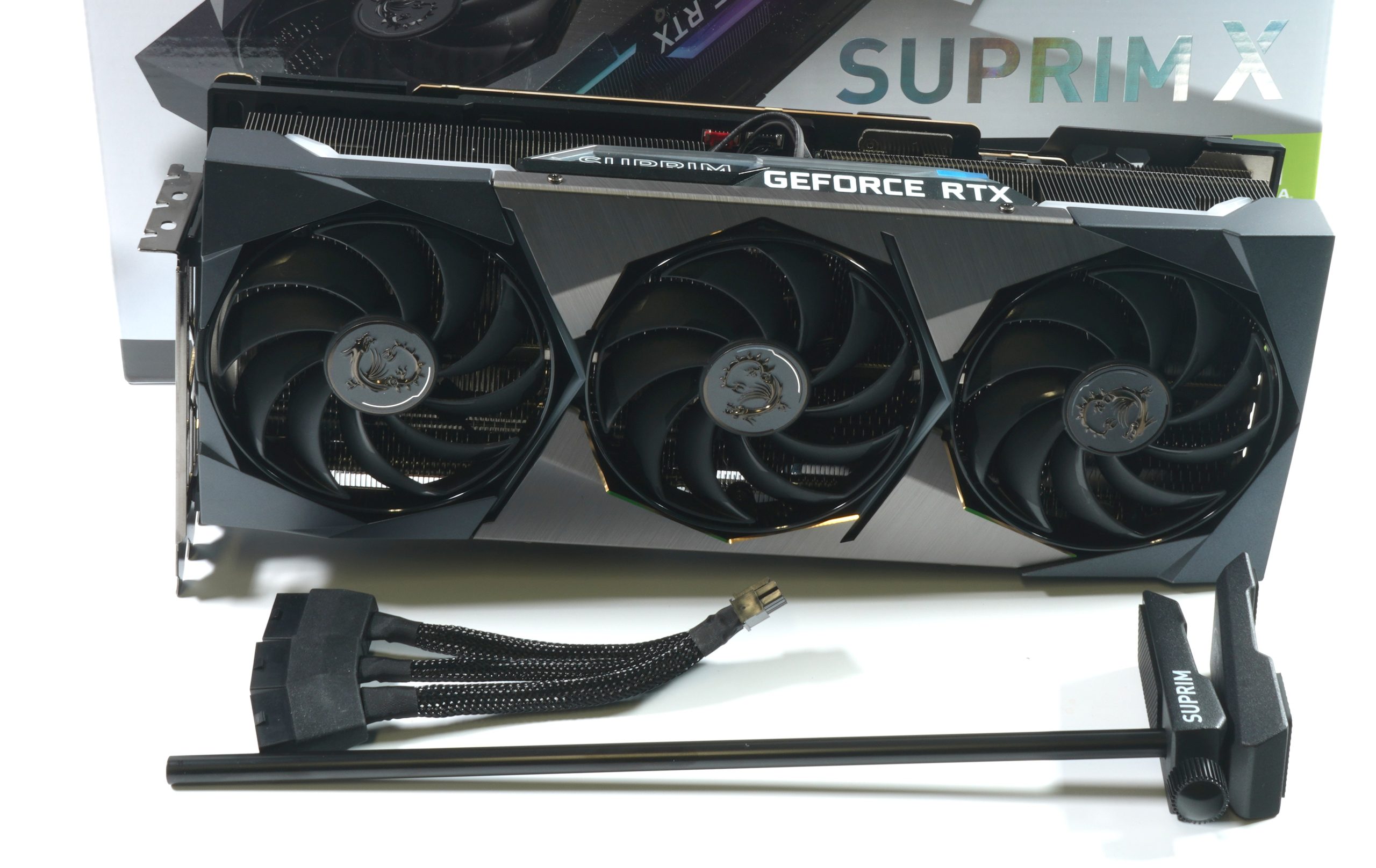
We see the already known adapter in the accessories, which breaks down the new 12+4 PCIe 5.0 connector to 3x 6+2 pins. You will find out in a moment what the included stand should be used for. Well, there is also a mouse pad free on the house, but that is more of a swag item. Furthermore, I will still test this card with the in-house 1000 watt power supply, but there will be an extra paragraph about that. The card offers a gaming and a silent mode, although I only used the gaming mode in the test so that the boost does what it is supposed to do. Otherwise, we could have stayed with the RTX 3090 without Ti.
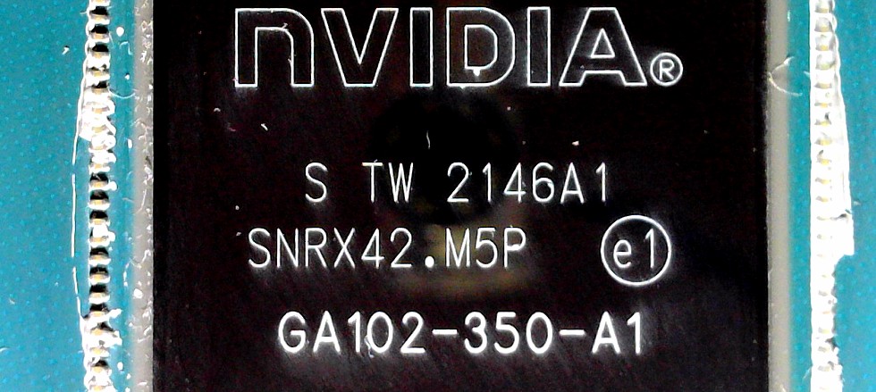
The uncut GA102-350-A1
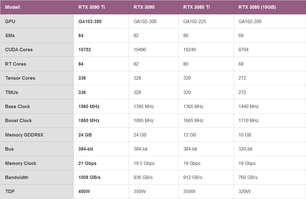
As described several times, the GA102 consists of graphics processing clusters (GPCs), texture processing clusters (TPCs), streaming multiprocessors (SMs), raster operators (ROPS), and memory controllers. The complete GA102 GPU contains 7 GPCs, 42 TPCs, and 84 SMs. The GPC is the dominant high-level hardware block that houses all the major graphics processing units. Each GPC contains a dedicated raster engine and now also two ROP partitions (each partition contains eight ROP units).
The GPC includes six TPCs, each containing two SMs and a PolyMorph Engine. The GA102 GPU also has 168 FP64 units (two per SM), which are not shown in the diagram below. The FP64 TFLOP rate is 1/64 of the TFLOP rate of FP32 operations. The small number of FP64 hardware units should ensure that all programs with FP64 code work correctly, including FP64 tensor core code.
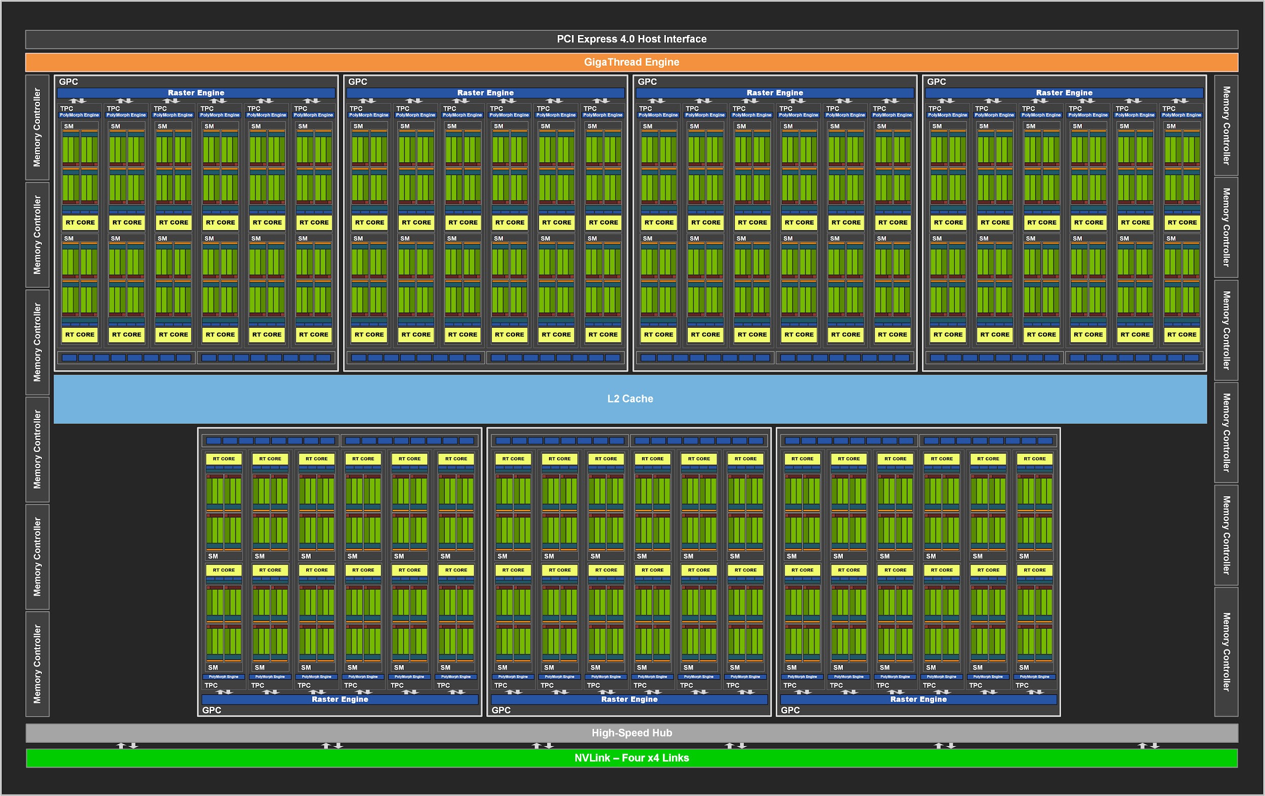
Each SM contains 128 CUDA cores, four third-generation tensor cores, a 256 KB register file, four texture units, a second-generation ray tracing core, and 128 KB of L1/shared memory that can be configured for different capacities depending on the compute or graphics workload requirements. The memory subsystem of the GA102 consists of twelve 32-bit memory controllers (384 bits in total). Each 32-bit memory controller is assigned 512 KB of L2 cache, so the GA102 GPU has a total of 6144 KB.
In the GA102, the ROPs are part of the GPC for the first time, which increases the performance of raster operations by increasing the total number of ROPs and eliminates throughput discrepancies between the scan conversion front-end and the back-end for raster operations. With seven GPCs and 16 ROP units per GPC, the GA102 GPU has 112 ROPs instead of the 96 ROPs previously available in a 384-bit memory interface GPU such as the previous generation TU102. This improves multisample anti-aliasing, pixel fill rate, and blending performance.

NVIDIA has given the GeForce RTX 3090 Ti a whopping 24 GB of GDDR6X memory in total, which is connected via a 384-bit memory interface. The GPU operates at a base frequency of 1560 MHz, which can be increased up to 1860 MHz (Boost), and the memory runs at 1313 MHz (21 Gbps effective). The fact that the boost can be significantly higher is no secret, and I will also log this under different loads. The TDP is 450 watts, but the board partners still have some leeway for more.
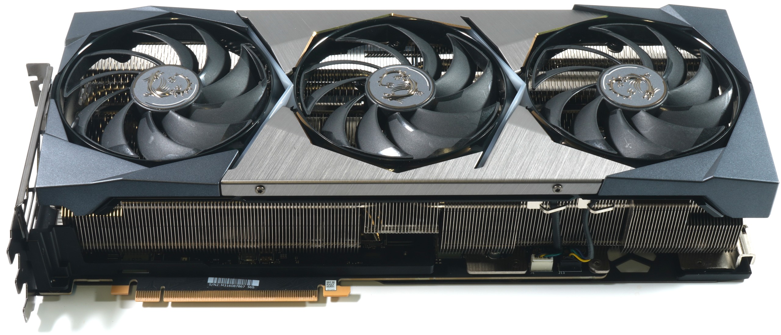
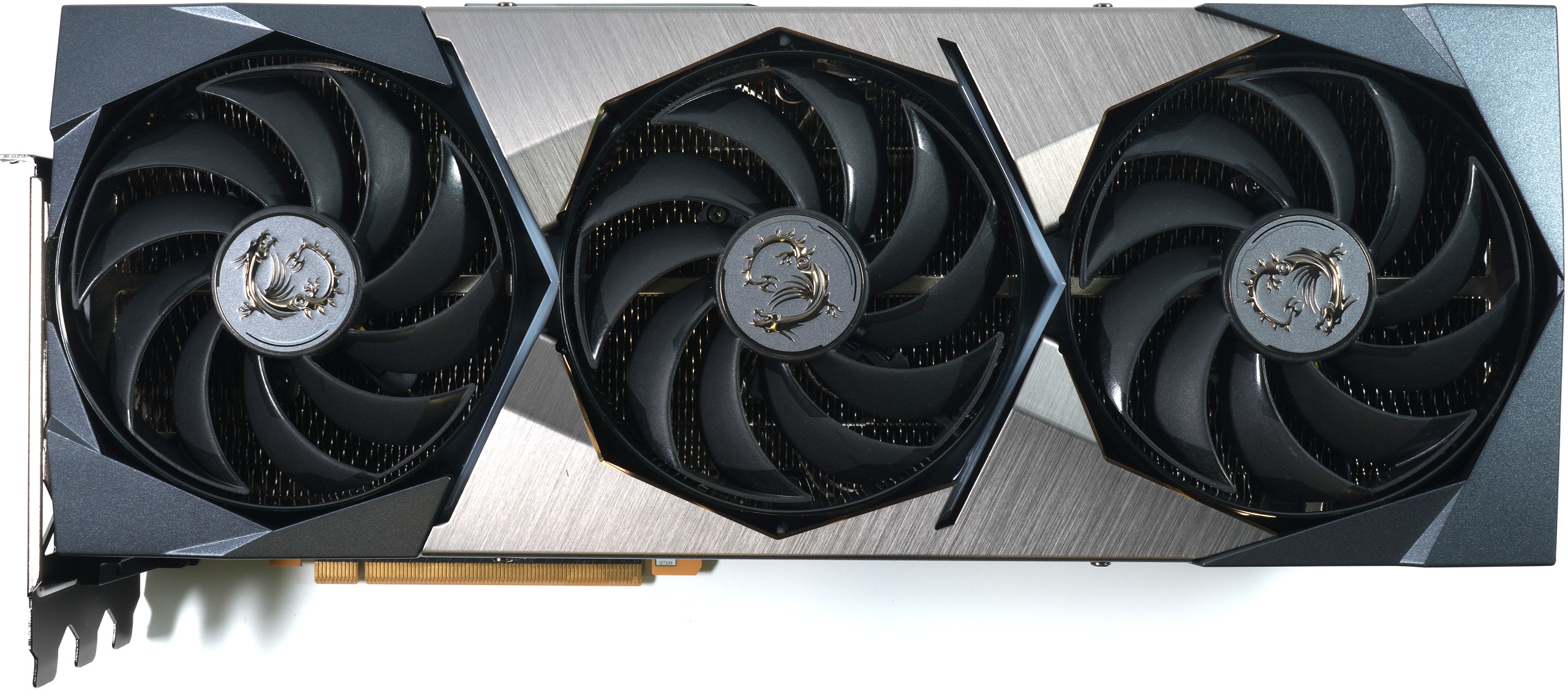
The MSI GeForce RTX 3090 Ti SUPRIM X 24 GB
The case of the card follows the well-known SUPRIM design language and is of course a real eye-catcher as a high-end model. Light metal for the cover of the brute cooler is just as natural as the implementation of various RGB light elements. With the SUPRIM lineup, MSI has managed to counter the older Gaming X lineup with a slightly more timeless card with no gaming frills, which is really pleasing. And the nice thing about all LEDs is that you can turn them off if you need to.
The design with the whopping 6.5 cm installation depth plus the 4 mm for the brushed aluminum backplate makes this card a real 3.5 slot design with all the known advantages and (in this case also many) disadvantages. The cooler overhang is trimmed for clearance in the backplate with large honeycomb openings. The backplate also contains the well-known LED logo with the finest LED beam power. In contrast to the predecessor models, the backplate is only screwed on from the back.
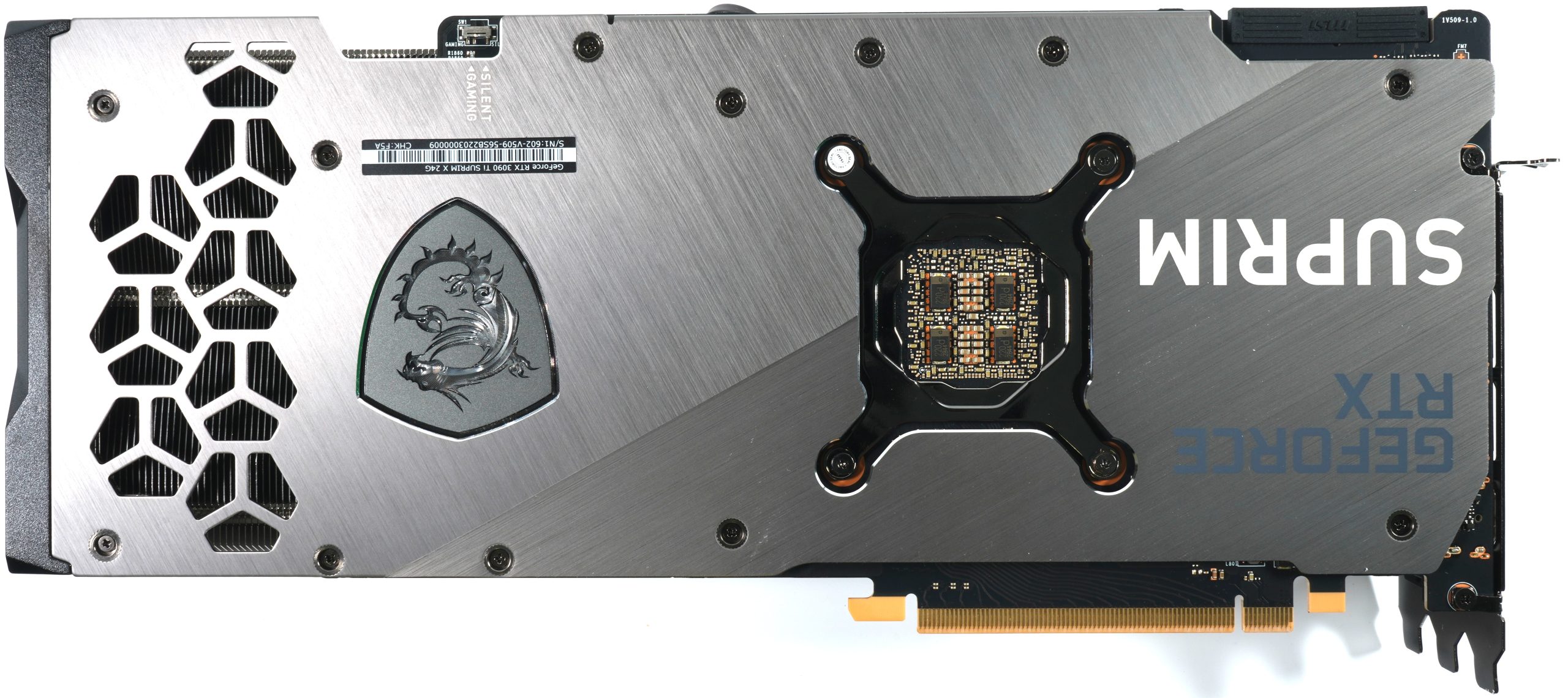
With its 2138 grams (without adapters and protective caps), the card is also a real super-heavyweight. The length of 33.8 cm is hefty and the installation height of 13.5 cm from the upper edge of the PCIe slot with the card installed to the top of the cover is also more than lush. It is thus one of the largest and heaviest cards in my collection and I have not only once relied on extra fasteners and the stand from the accessories in order not to destroy the motherboard (slot).
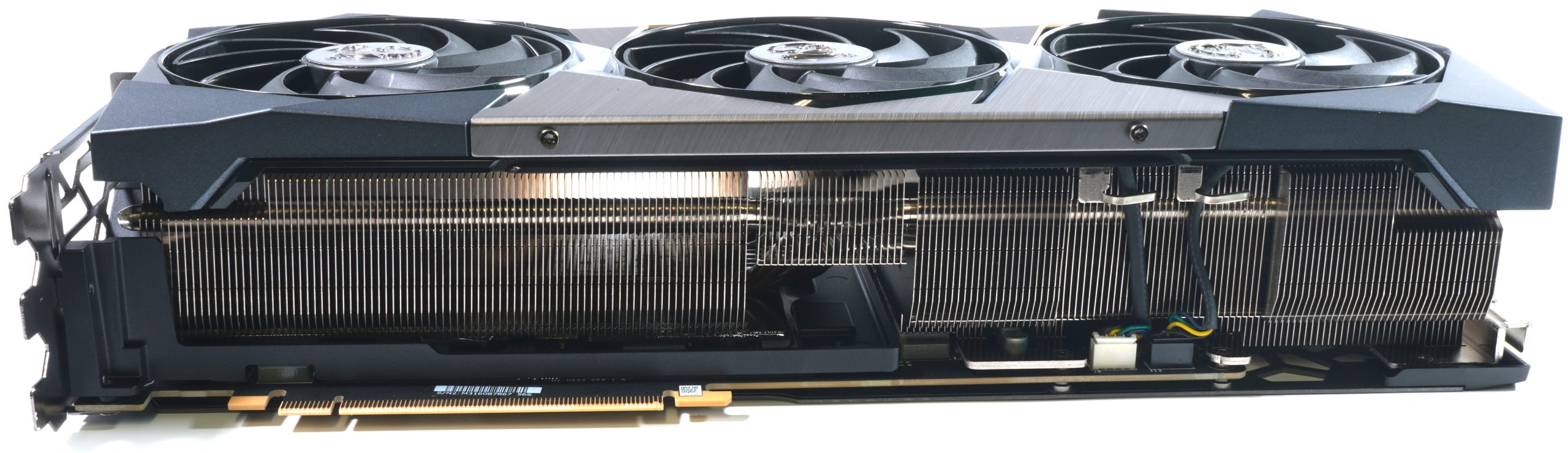
The single, new 12+4 pin connector on the top is quite sufficient and it also visually marks the end of the hidden pcb behind it. You’ll see on the next page that the extra-long cooler adds a lot to the picture, even though the PCB alone is already quite large. But the three fans also need to be accommodated. On the top, we see the RGB-lit SUPRIM and GeForce lettering, along with the usual light strips.
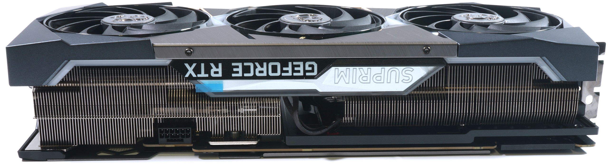
The HDMI 2.1 port should not be missing, and of course the three current DisplayPorts. The 3-slot panel is huge and the monstrous bracket is still topped by the cooler assembly. In the end, four slots are already occupied here and the card will eat up every Mini-ITX board with relish.

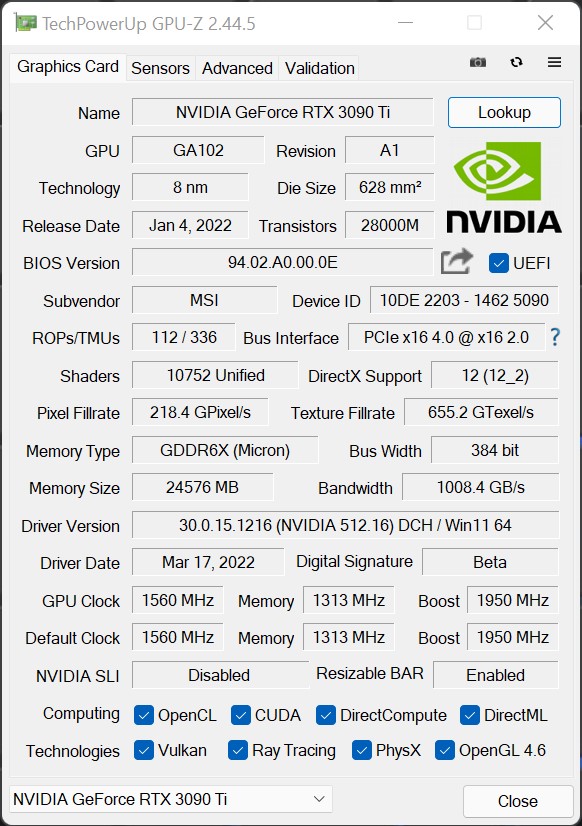
The data of the tested MSI graphics card is once again shown in the current GPU-Z screenshot, the rest I already mentioned above. The 1560 MHz base clock corresponds to NVIDIA’s reference specification and MSI raises the boost clock to 1950 MHz ex-factory. The 1313 MHz memory clock was to be expected and the memory expansion with 24 GB on the 384 bit interface is logically as well, when you think of the 12 memory controllers with 32 bits each from the schematic shown above. After all, this is enough for a memory bandwidth of 1008.4 GB/s.
Again, I have a table for all statisticians among you:

- 1 - Introduction, Unboxing and Technical Data
- 2 - MSI's PSU, Test System and Test Methods
- 3 - Teardown, PCB Analysis, Components and Cooler
- 4 - Gaming Performance (Bars)
- 5 - Gaming Performance (Curves)
- 6 - Percentiles (Curves)
- 7 - Frame Times (Curves)
- 8 - Frame Times (Bars)
- 9 - Variances (Bars)
- 10 - Power Draw GPU in Detail (Each Game)
- 11 - Power Draw CPU in Detail (Each Game)
- 12 - Effiziency in Detail (Each Game)
- 13 - Power Consumption in Games and Applications (Average)
- 14 - Transients, PCIe Standard and PSU Recommendation
- 15 - Temperatures and Thermal Imager
- 16 - Fan Speed, Noise, Coil Whining
- 17 - Summary and Conclusion


52 Antworten
Kommentar
Lade neue Kommentare
Urgestein
Mitglied
1
Urgestein
Moderator
Veteran
Urgestein
Mitglied
Urgestein
Veteran
Urgestein
Urgestein
Veteran
Mitglied
Urgestein
Urgestein
Urgestein
Veteran
Mitglied
Alle Kommentare lesen unter igor´sLAB Community →