


Board analysis and power supply
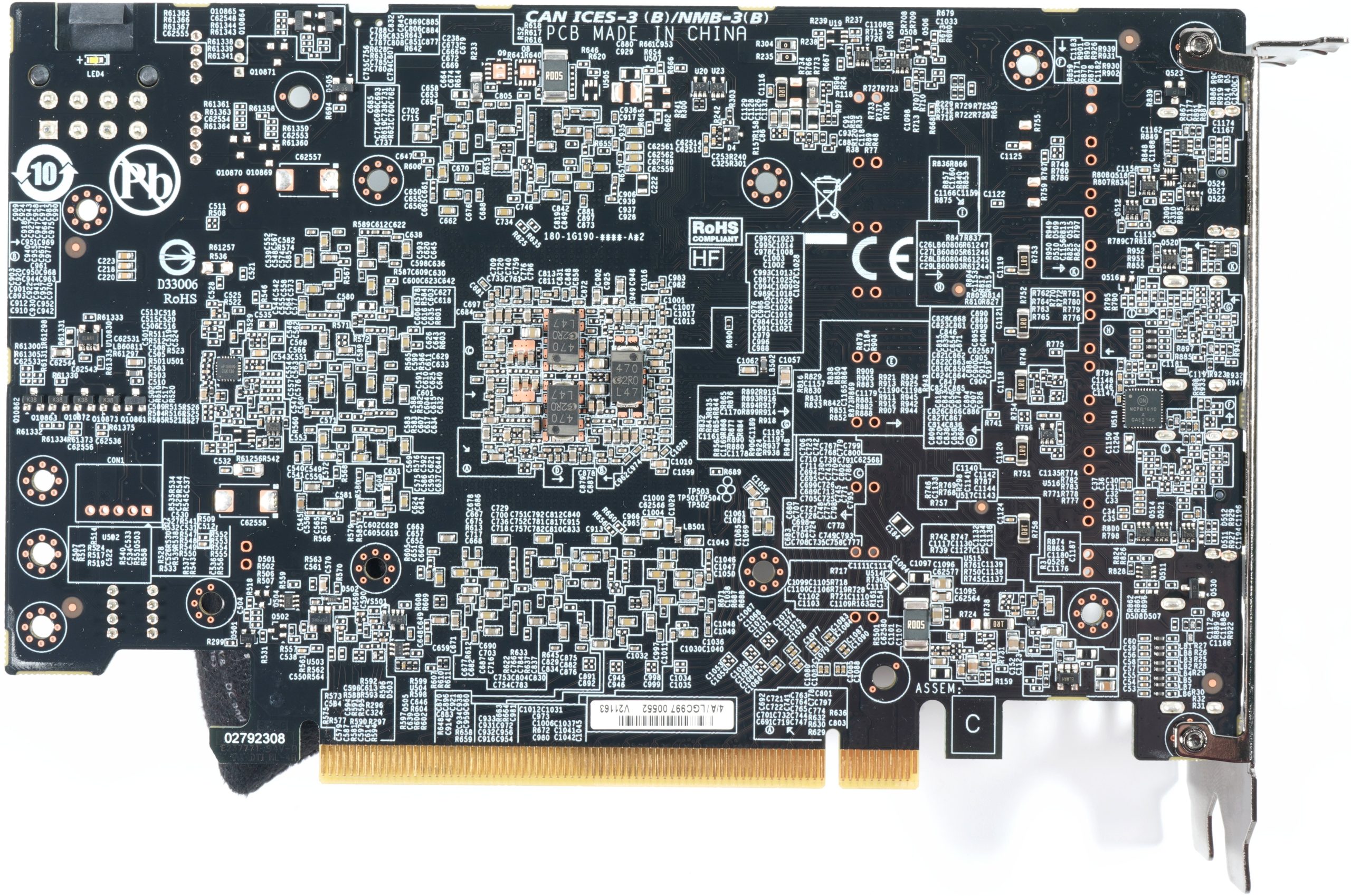
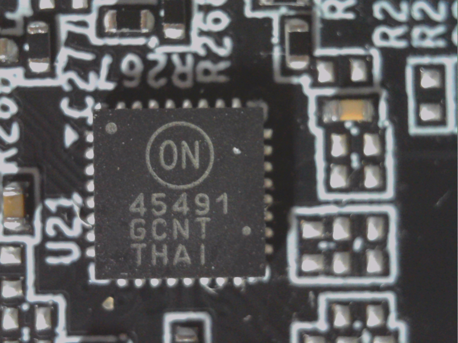
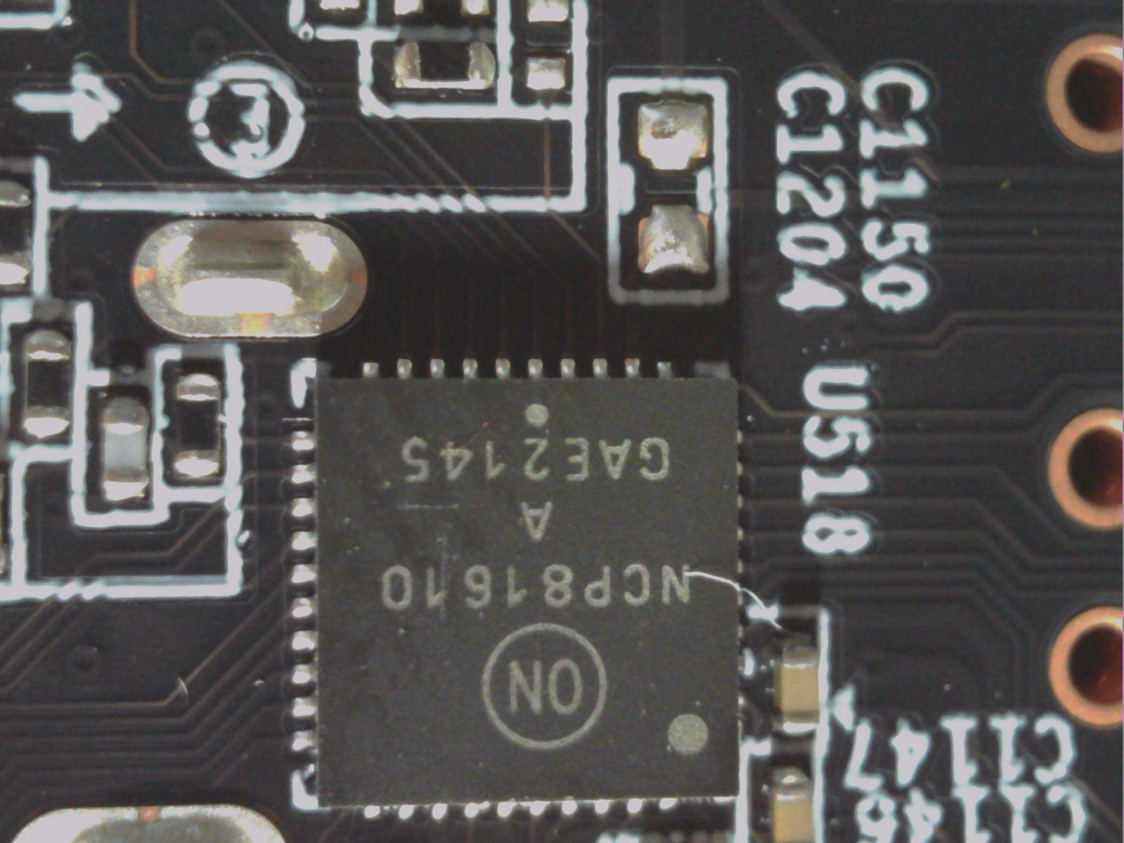
The card has the same multi-layer board without the more complex backdrill process as the GeForce RTX 3060 Gaming OC. The type of power supply is well-known and was only shortened a bit more for the RTX 3050 (which can be seen well in the empty spots). Here, there are still a total of five individual phases (one more than with Palit, a maximum of 8 would be possible), which are provided by an NCP81610 from On Semi on the back. This is a rather cheap digital PWM controller with VID interface, compatible with NVIDIA’s Open VReg specification.
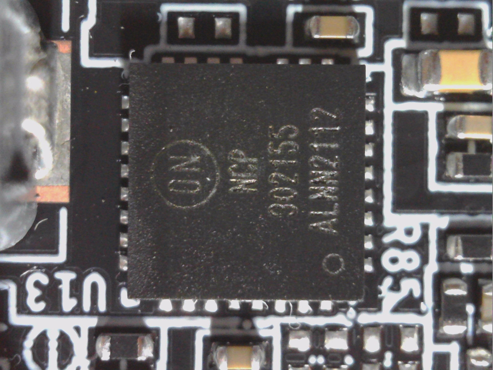
These five phases are each implemented with On Semiconductor’s low-cost DRMOS NCP302155 (55 amps max.), which does not enable MOSFET DCR, but at least still provides temperature protection circuitry. However, the five phases used here hardly proceed more efficiently than the four phases on Palit’s Dual OC, so there are also various losses. The power dissipation saved in this way should actually have been available to the GPU, since the TDP corset of the cards is the same and is measured at the ports. So any loss on the card is at the expense of the GPU. Unfortunately, Gigabyte gives away some potential here, because the card is hardly faster than Palit’s Dual OC despite higher power consumption.
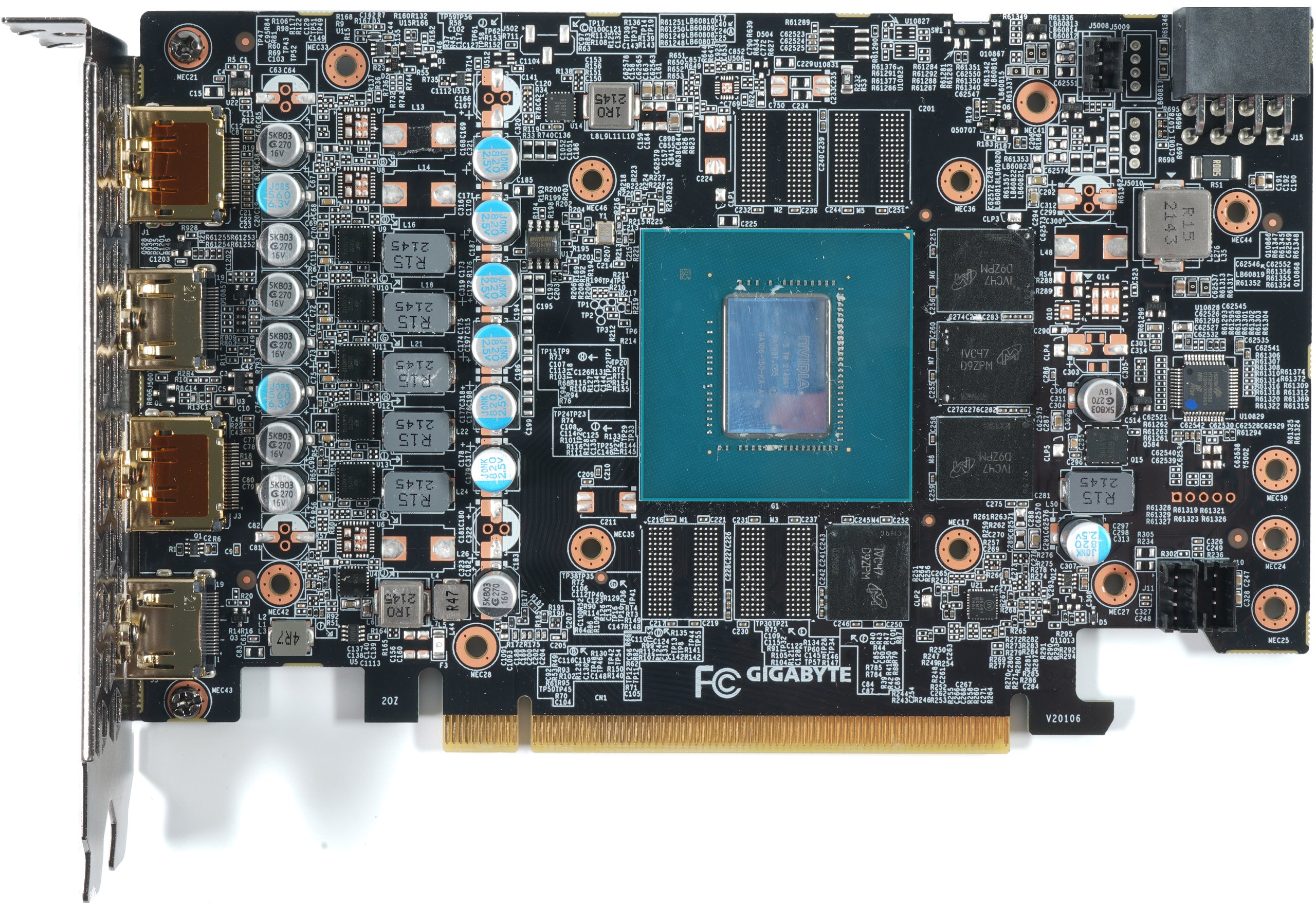
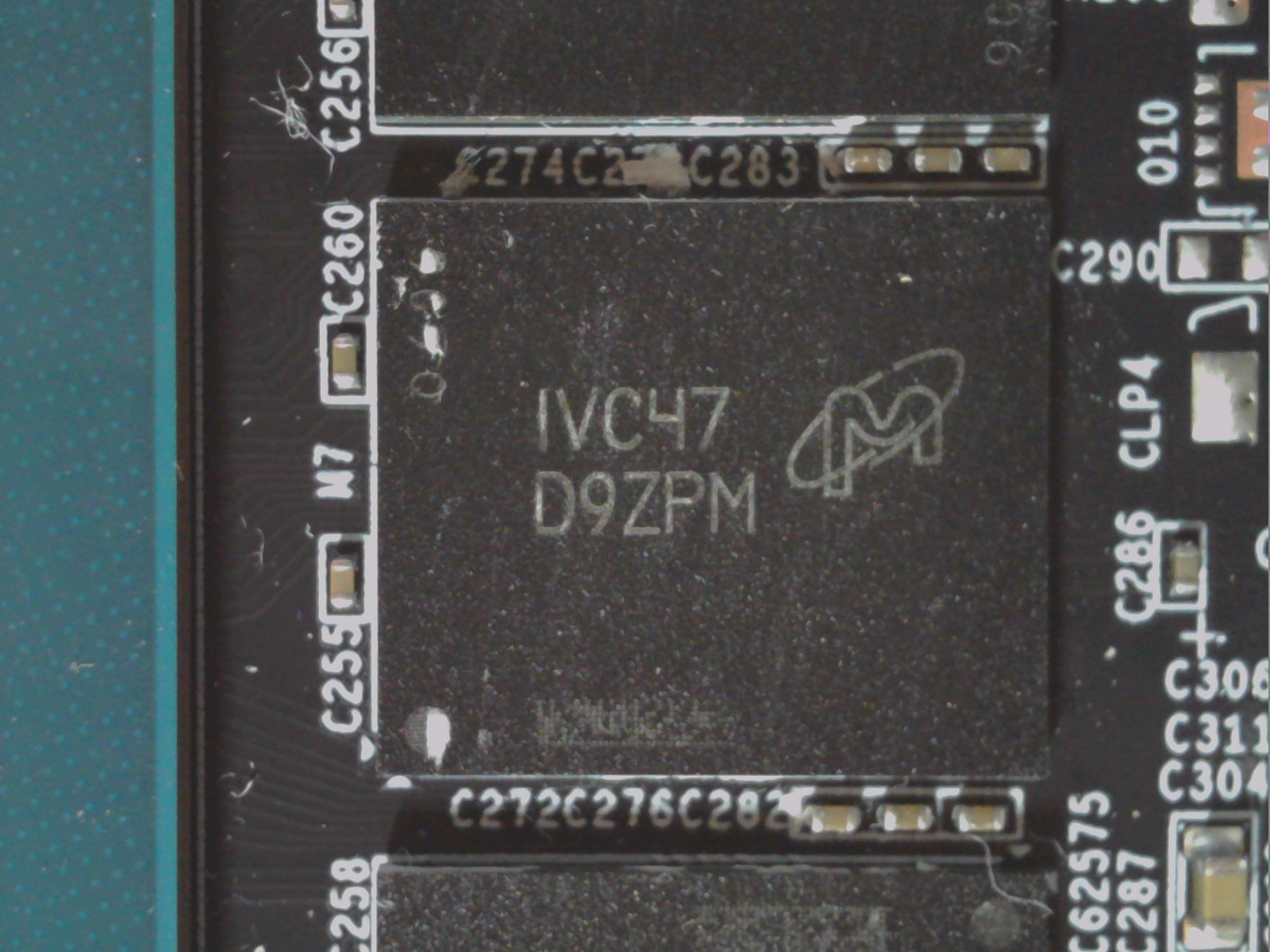
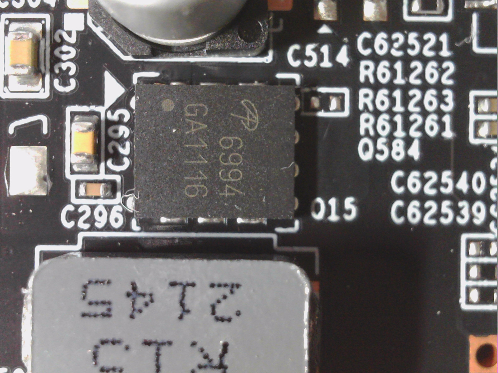
Gigabyte also doesn’t use a polyphase converter for the more frugal GDDR6 memory from Micron in the form of four 2GB modules (D9ZBM), but a simple step-down converter with discrete placement, whereby a rather cheap solution with an asymmetrical AON6994 dual N-channel MOSFET from Alpha & Omega instead of a PowerStage behind a uP1666Q from UPI (back) is also used here. The second possible phase has simply been saved on the card (empty space on the right above the one phase under the 8-pin socket).
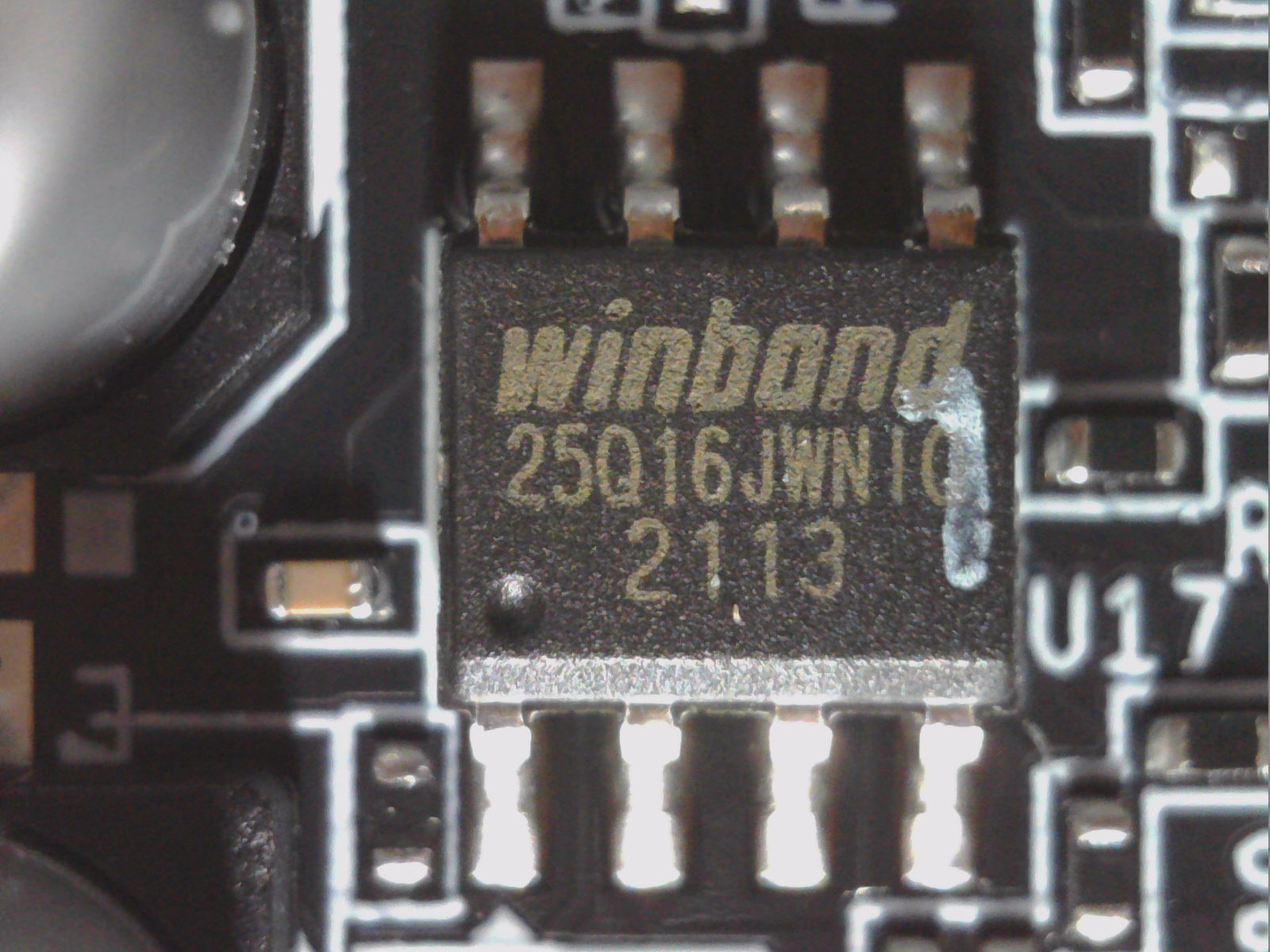
This simple assembly is also used for further partial voltages on the board, which by the way is completely sufficient. On the front, there is still a simple single UEFI EEPROM to discover, while the backside doesn’t show any interesting assembly variations except for the two PWM controllers and some small MOSFETs.
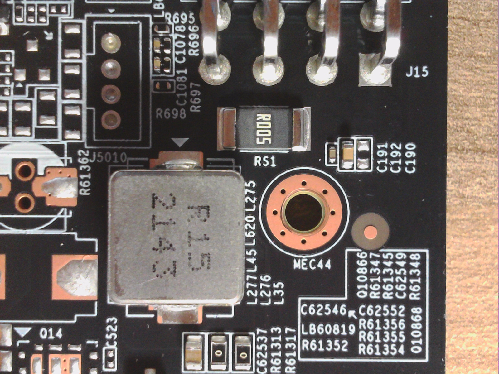
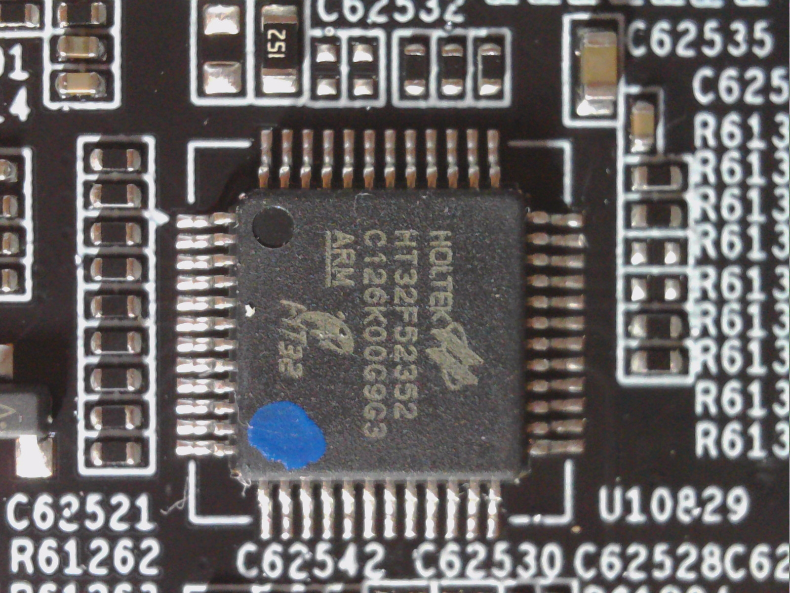
For input smoothing one coil with 1 µH (front side) is used behind which a shunt (rear side) is placed for the 8-pin connector as well as for the PEG motherboard slot together with a 20A fuse. The voltage drop of the shunt is used to measure the flowing currents. A simple ON Semi chip is used for this. LTE’s small MCU handles the RGB lighting and fan control. That’s about as exciting as it gets. The following pictures show the mentioned components once again in detail:
Cooler and disassembly
The front is dominated by three 7.6 cm fans (8 cm opening) with 11 rotor blades each, which do not act particularly quietly and correspond to those on the other cheap Gigabyte models. There are no more special features to observe from above for the time being. The cooler cover sits on top of the cooler and it is virtually only supported via the screw connection of the GPU and the coil heatsink.

Disassembly is simple. After unscrewing half of the screws of the backplate and the GPU heatsink, the cooler can also be removed completely quite easily. You just have to disconnect the two fan cables and the RGB lifeline. The extremely thick, very soft and also sticky pads on the memory modules and the VRM ensure that even possible manufacturing tolerances of the package of up to 0.5 mm in height can still be easily compensated.
We only see two, not 6 mm heat pipes made of copper composite material, which were ground above the GPU (Direct-Heat-Touch) and pressed into the surrounding aluminum heat sink and which then, each on one side, cool the block via GPU and VRM on the one hand and transport the waste heat to the card’s end on the other hand. However, this is not really efficient, but rather cost-down. The memory is cooled by the aluminum heatsink via the thick pads, the voltage converter coil heatsink sits separately. The coils are therefore actively cooled here. The MOSFETs only rest on the bent fins of the cooler. Unfortunately, one voltage converter phase remains uncooled and could at least have been thermally connected to the fin cooler with a thick pad on the back.
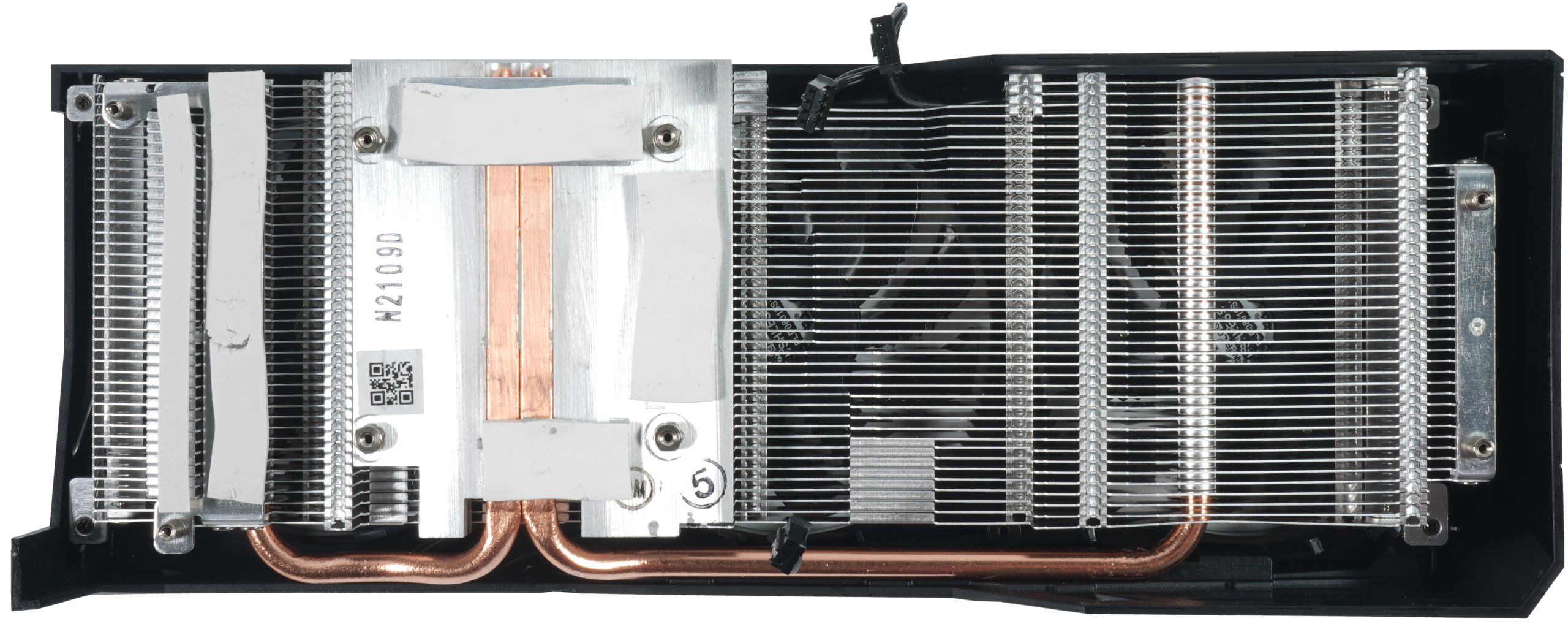
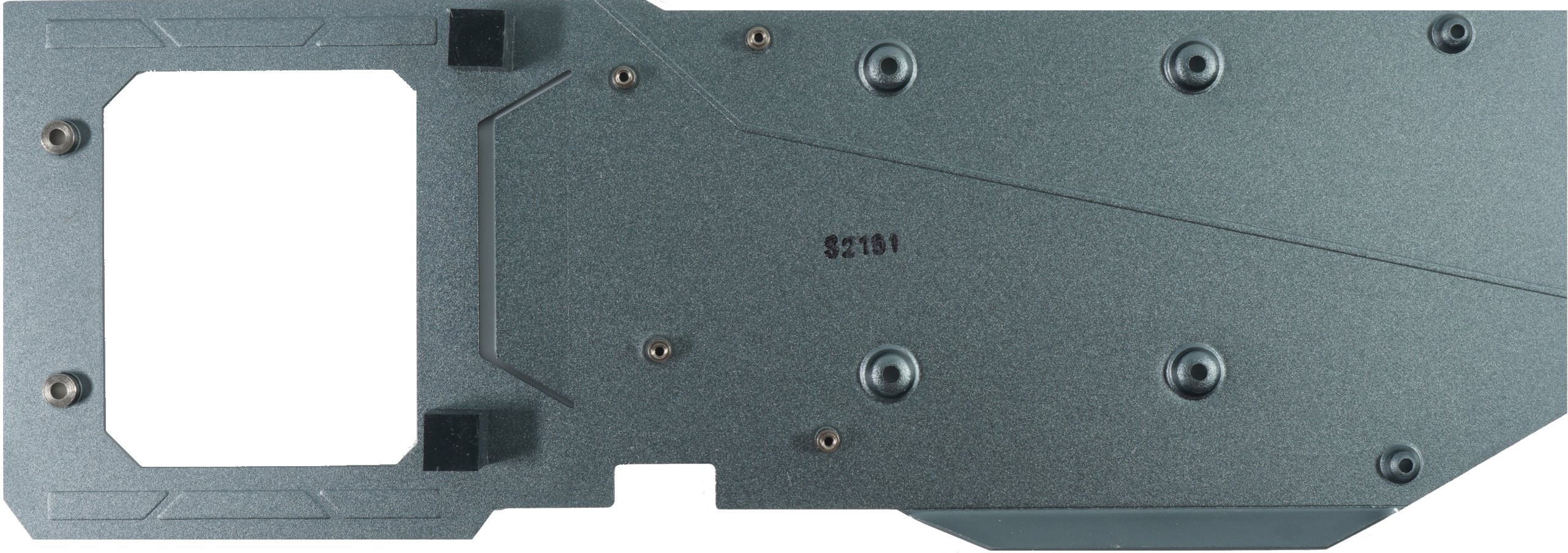
On the back, you’ll find a backplate made of light metal, which unfortunately doesn’t have any cooling function at all and thus once again only serves to look good and stabilize the cooler assembly together with the PCB. That’s all it can do.


25 Antworten
Kommentar
Lade neue Kommentare
Veteran
Urgestein
Urgestein
1
Veteran
Urgestein
Urgestein
Urgestein
Urgestein
Urgestein
Urgestein
Urgestein
Veteran
Mitglied
Mitglied
Veteran
Urgestein
Alle Kommentare lesen unter igor´sLAB Community →