


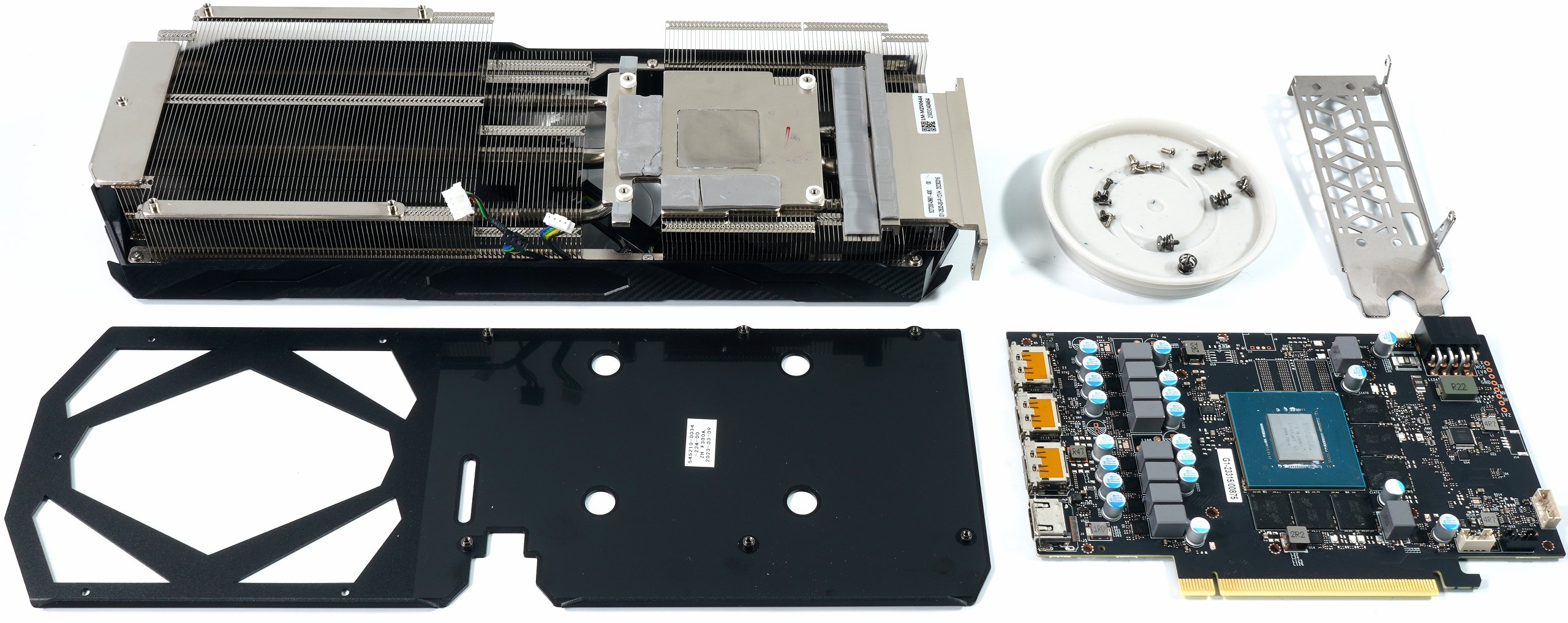
Teardown
The KFA2 GeForce RTX 4070 EX Gamer 12 GB isn’t disassembled quite as quickly, because the screwing of the backplate is also done from the front. This makes disassembly a bit more involved, especially since you also have to pull off three connectors instead of two (2x fan and LED). But they came off relatively easily, but without the danger of simply slipping out on their own. The slot bracket is screwed between the PCB and the backplate and locked extra at the cooler. I’ll explain why in a moment.
PCB layout and components
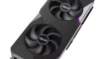
Let’s first start, as always, with the PCB of the KFA2 GeForce RTX 4070 EX Gamer 12 GB. NVVDD is still the main voltage and you even use a voltage converter design with a total of 8 true phases (instead of 6 on the FE and many MSRP cards) and the resulting 8 control loops for NVVDD alone. So, you save quite a bit compared to the RTX 4070 Ti, but this is still acceptable considering the significantly lower TDP.
Nevertheless, the card has an interesting peculiarity, because the voltage converter, which is positioned individually above the unpopulated RAM slots in all other cards (including the FE), is completely omitted. It is replaced by an additional DrMOS placement at the bottom left of the NVVDD voltage converter row. This has an advantage and a disadvantage. Advantage: The cooler becomes simpler (heatsink can be shorter) and thus cheaper. Disadvantage: This phase is connected to the motherboard slot, which significantly increases the current flow there.
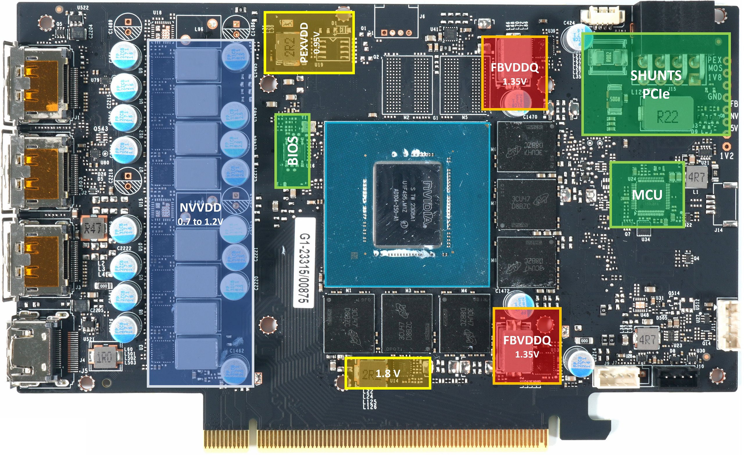
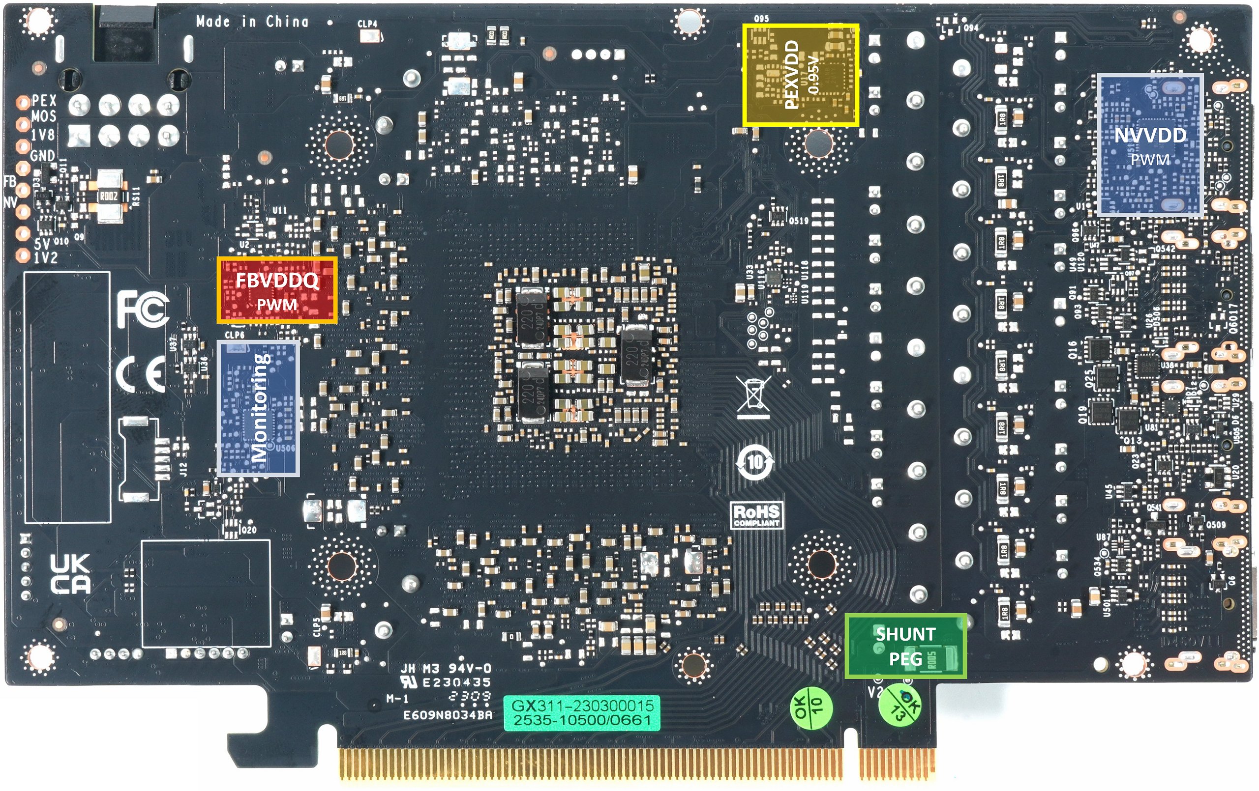
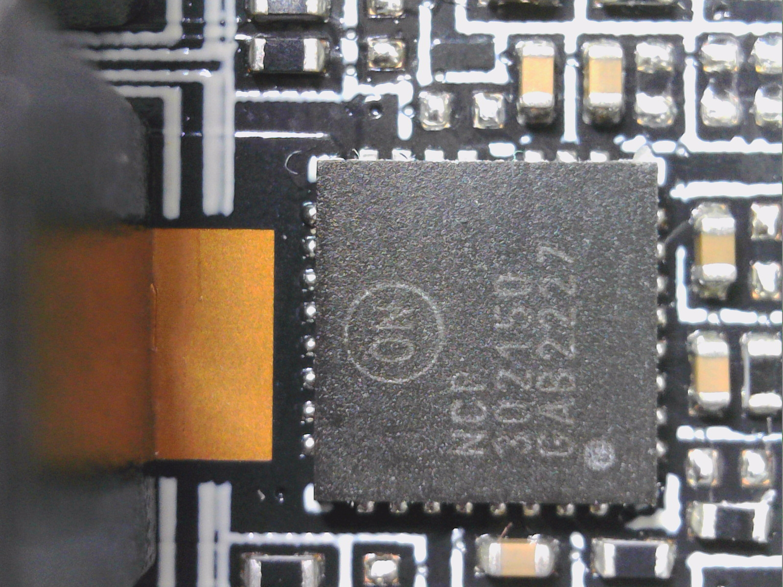
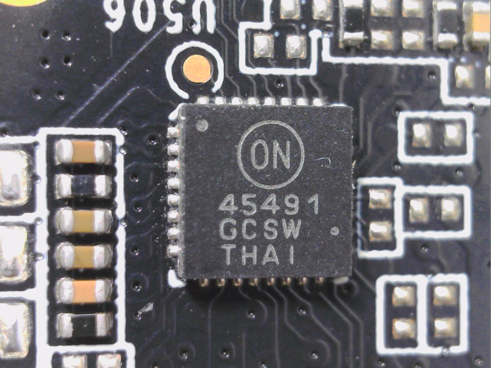
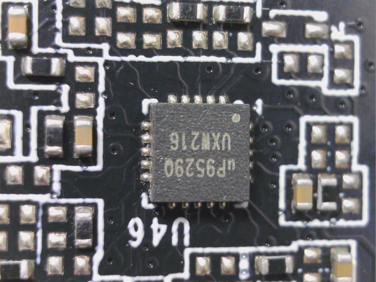
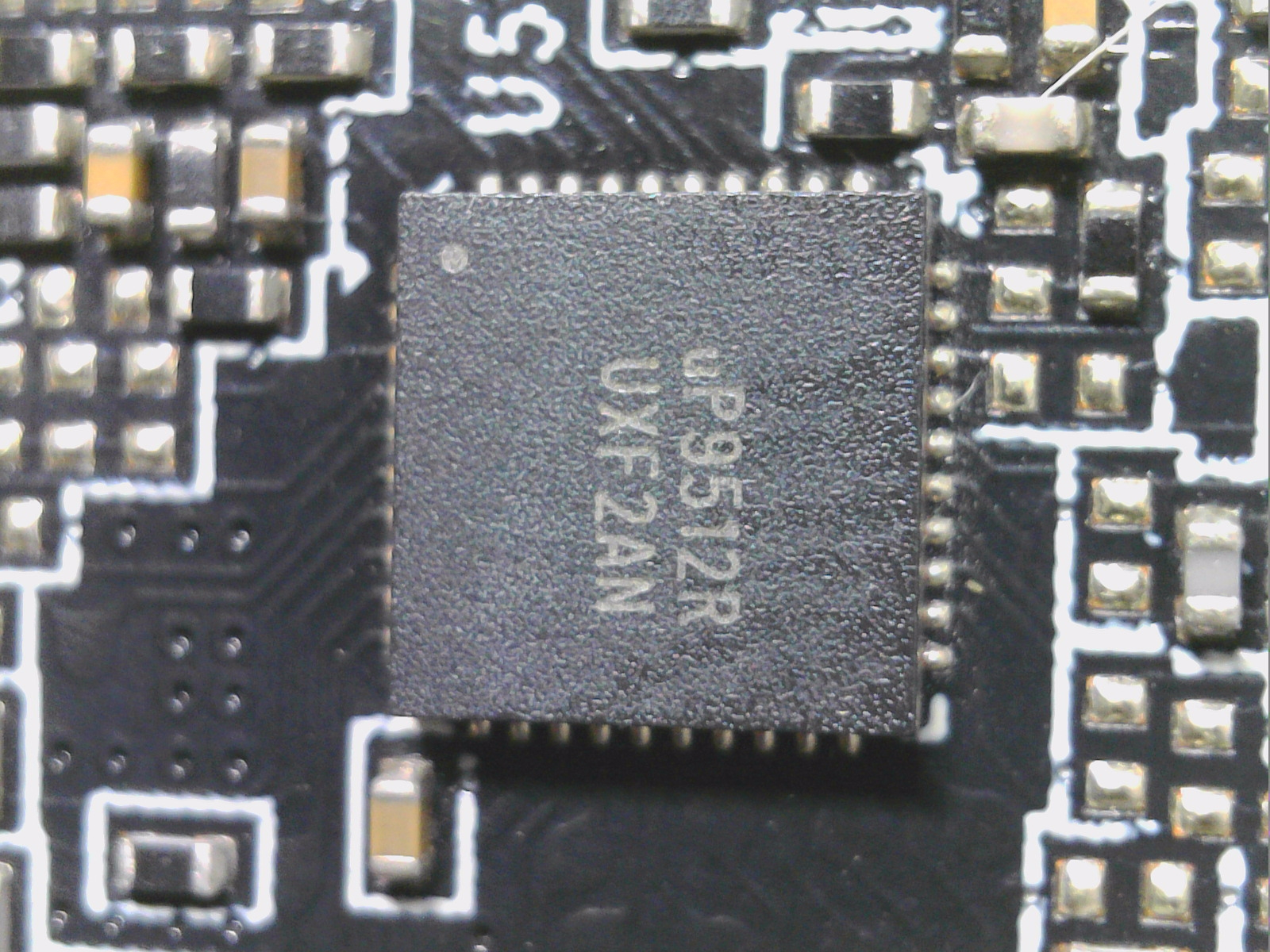
In the end, however, it all looks just as meager as the FE, which may be ok considering the price. One also uses separate PWM controllers for NVVDD (GPU core) and FBVDDQ (memory), because the top models among the PWM controllers are unfortunately much too expensive. Therefore, the good and well-known uP9512R from UPI Semi has to do the job again, which can easily generate the 6 phases and is significantly cheaper than the models from Monolith, which, however, is completely sufficient. A second PWM controller in the form of the small uP9529Q controls the two phases for the memory. Both controllers are located on the backside of the board. Directly in between there is a uPI uS5650Q for monitoring the four 12V rails (3x Aux and 1x PEG).
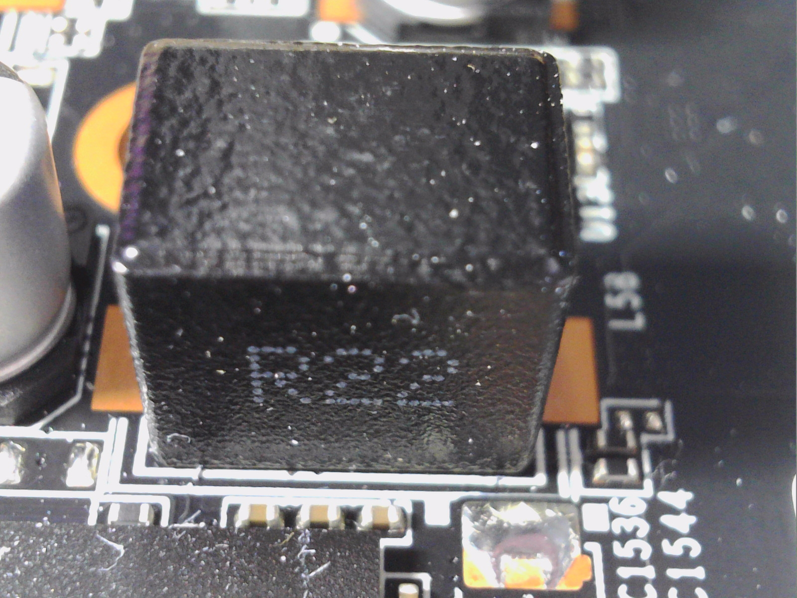
All used DrMOS, also those for the memory, are rather cheap products from Alpha & Omega, which we already know from the Founders Edition. The AOZ5311NQI-03 with 55 A peak current used in all control circuits for NVVDD and FBVDDQ (memory) integrates a MOSFET driver, a high-side MOSFET and low-side MOSFET in a single package. This chip is specifically designed for high-current applications such as DC-DC buck power conversion applications. This integrated solution reduces board space requirements compared to a discrete component solution. The coils used for NVVDD and the memory have an inductance of 220 nH, and the capacitors are in cup form, which is less expensive.
And I want to (and must) say a word about the popular lists, which are often used on the Internet to evaluate the graphics card components and which only refer to the DrMOS used in each case. These lists are worthless and even misleading as long as you don’t know the used switching frequency of the voltage converter, the actual temperatures and flowing currents and evaluate them in context. The maximum values in the specifications are far away from what occurs on a card in practical operation. This can, despite the same DrMOS, even turn out extremely different in the evaluation from card to card and one must already consult the measurement curves and not theoretical final values.
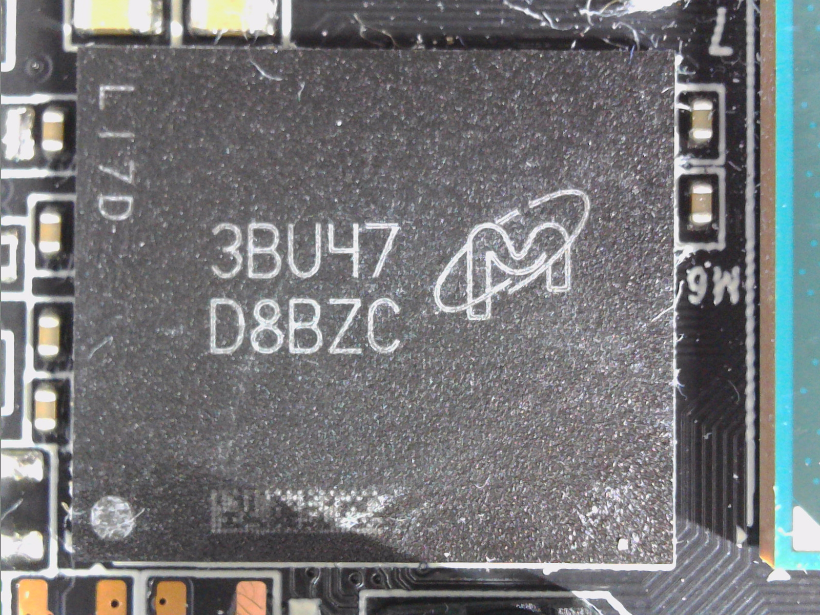
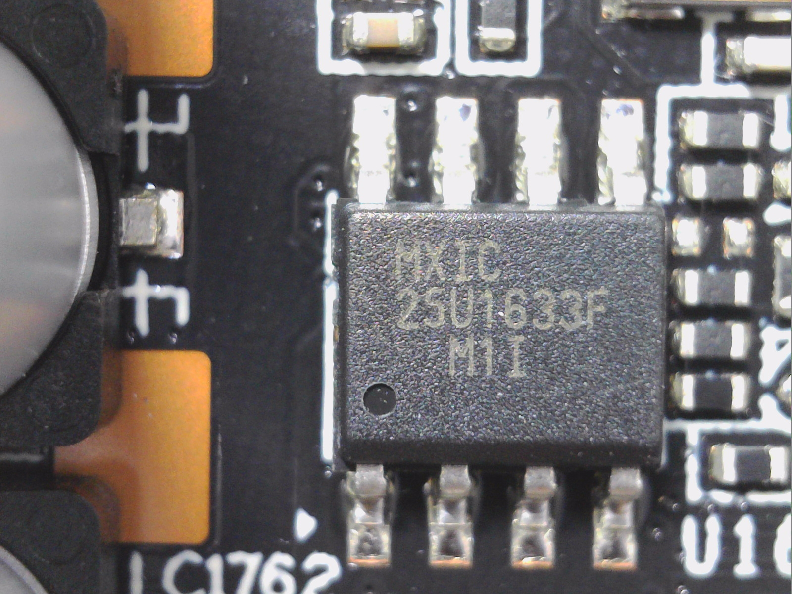
The 12V rails on the 8-pin connector are combined into a single rail directly after the socket, another one is connected to the PEG and is only slightly used for NVVDD. The BIOS is in the usual place and the generation of the rest of the extra-low voltages is as usual. The GDDR6X memory chips are manufactured by Micron and bear the model number D8BZC, which is decoded to MT61K512M32KPA-21:U. They are specified for a clock frequency of 1313 MHz (21 Gbps GDDR6 effective). There are no more special features.
Teardown: The cooler
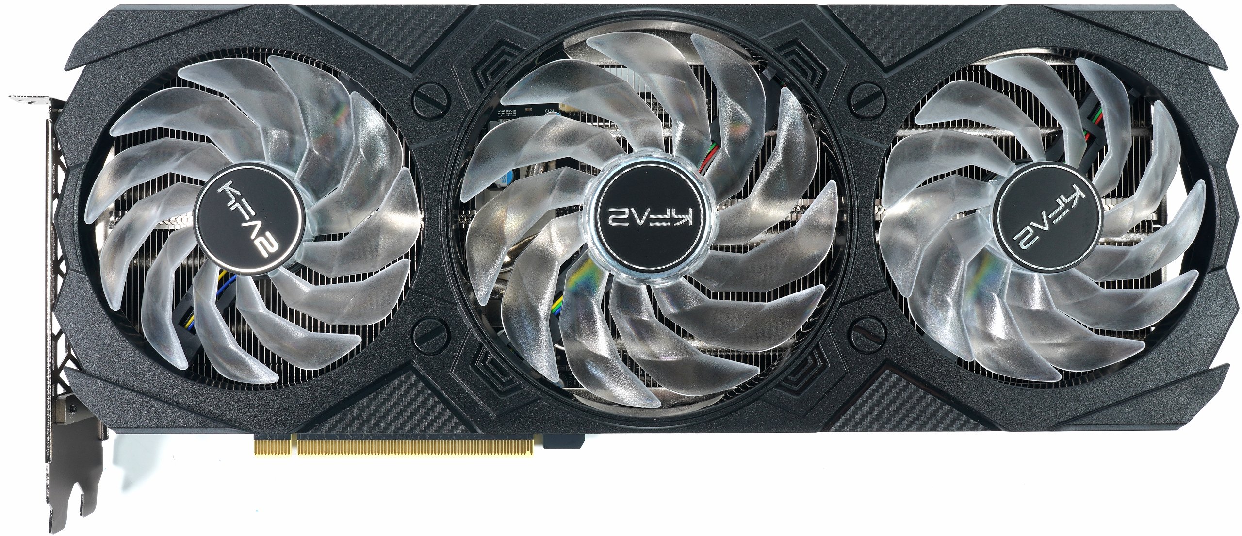
KFA2 relies on the usual cheap RGB fans, in this case even three. Two fans, each with a 9 cm rotor diameter (opening 9.2 cm), flank a centrally located 10 cm fan (opening 10.2 cm). All fans have 11 rotor blades each without a circumferential ring, which emits a rather wide airflow towards the radiator and also leads to more turbulence and losses at the air intake and below the radiator cover (tear-off noise). The engine is a wee bit growly, but I’ll get to that later.
A total of three nickel-plated heatpipes (2x 6 mm, 1x 8 mm) made of copper composite material lead from the heatsink to the end of the cooler, part of which also protrudes over the very short PCB. Here it comes then to a gladly seen “draught”, since no circuit board can brake out the air flow. All heatpipes also lead towards the slot bracket. This is also where the VRM heat sink is located, which is much more stable compared to the MSI RTX 4070 Ventus and does its job very well. The two voltage converters for the memory are also actively and validly cooled by cooling surfaces on the large GPU heatsink.
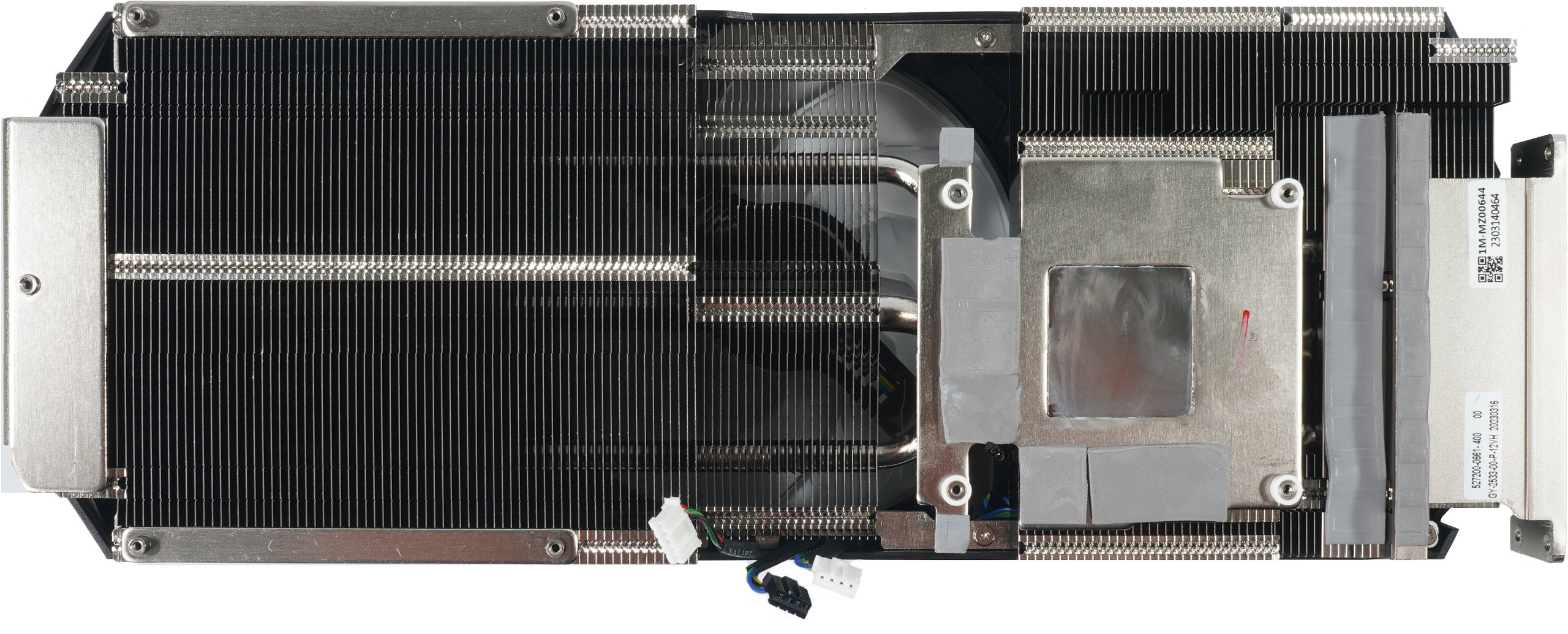
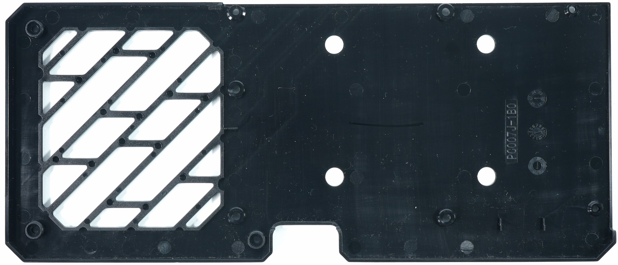
The used pads are okay, but not from the top shelf. Thus, you’ll find a bit of cost-down here as well. The light metal backplate is screwed to the cooler cover and the PCB. This stabilizes the board almost perfectly and prevents it from bending in the horizontal setup. I already wrote something about the airflow and we can see the appropriate cutout for it here (left in the picture).
And now we come back to the slot bracket, as promised. Since the slot bracket is firmly connected to the PCB and the backplate, KFA2 even stabilizes this bracket with four screws additionally with the cooler cover. This guarantees a consistently good contact pressure on the areas to be cooled (VRM).

- 1 - Introduction, technical data and technology
- 2 - Test System and the igor'sLAB MIFCOM-PC
- 3 - Teardown: PCB and components, cooler
- 4 - Gaming performance
- 5 - Details: Power consumption and load balancing
- 6 - Transients and PSU recommendation
- 7 - Temperatures, clock rates and infrared analysis
- 8 - Fan curves, noise and audio samples
- 9 - Summary and conclusion


96 Antworten
Kommentar
Lade neue Kommentare
Veteran
Urgestein
Mitglied
Urgestein
Veteran
1
Urgestein
Moderator
Mitglied
Mitglied
Mitglied
Mitglied
Mitglied
Mitglied
Mitglied
Alle Kommentare lesen unter igor´sLAB Community →