


Real measured values in the memory module
Interestingly, Micron was completely silent on the NVIDIA-exclusive GDDR6(X) for now, as even the “Device Thermal Information” included with the GDDR6 documentation annoyingly still ends at GDDR5. On inquiries among colleagues e.g. from the R&D departments it was unanimously said that the maximum temperature Ttot before the beginning of a possible destruction of the chip should be at 120 °C and Tjunction is probably specified at 105 °C for the GDDR6 or even at 110 °C for the GDDR6X as maximum value. But first let’s have a look at the thermal scheme of such a GDDR6X module, because I can’t spare you a little bit of theory at this point. Interesting at first is PT, i.e. maximum “power” Ptot, which is supplied as electric energy and also almost completely given off again as heat (see red arrow).
That should be around 2.5 to 3 watts per module, which doesn’t sound like much at first, but due to the small structure width and heat density (density) it is quite a house number, especially if the board underneath is already quite hot. Because even though the memory module may look quite large as a package: the chip itself is rather tiny. You just need a lot of space for all the ports and besides, you’d like to stay backwards compatible:
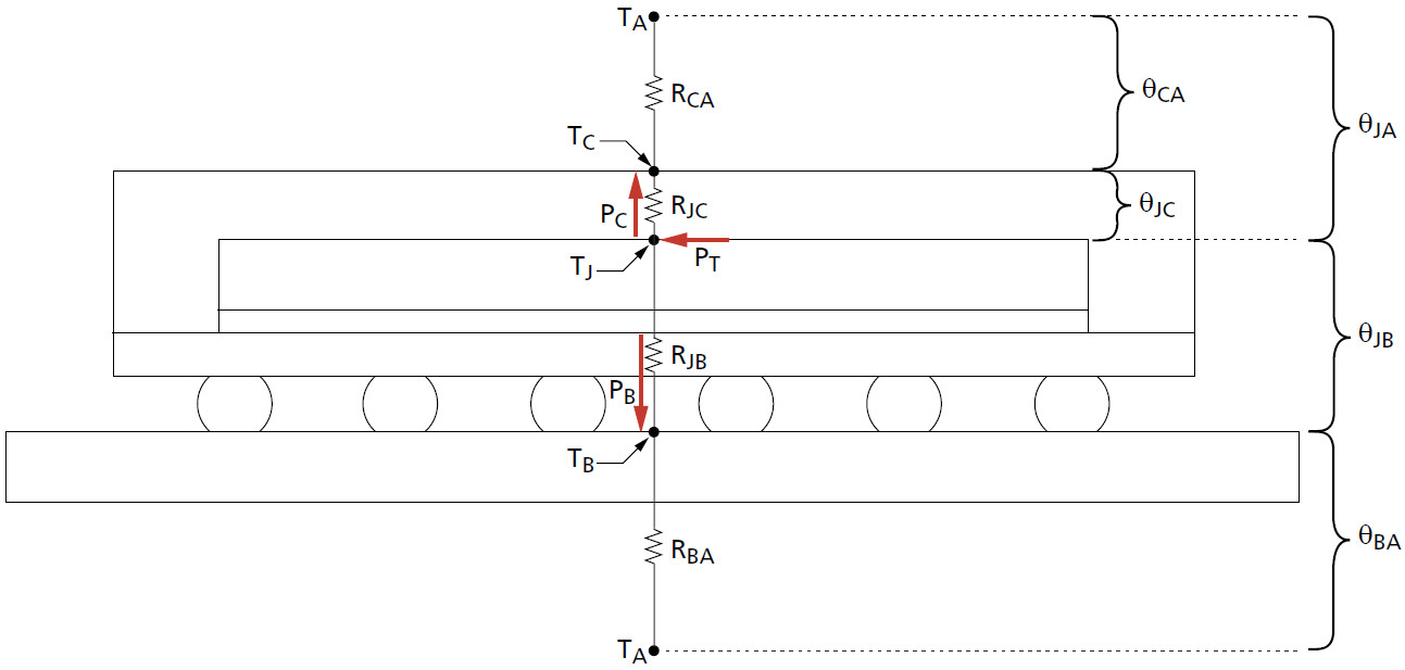
At the same point TJ, i.e. Tjunction now comes into play. Maximum chip temperature and maximum power dissipation are therefore directly related here. This is also exactly the value that e.g. AMD also outputs as memory temperature in the sensor loop. I asked AMD at that time and found out that it is not an average value of all modules, but the absolute peak value, i.e. Tjunction of the hottest module of a card. Important are also the values PB marked with the other two red arrows, so as Pboardthe power dissipated through the board and PC, which stands for the dissipated heat Pcase through the top of the case (package).
In addition, there are all occurring thermal resistances of the individual layers and the combination of related layers as a directional value upwards and through the board downwards, as well as the temperatures of the environment (air) TA or Tair at the top and bottom, whereby both can also deviate if cooling is carried out on one side. I already wrote that you can only indirectly consult the temperatures measured NEXT to such a memory module on the board when it comes to the temperatures INSIDE. The temperatures of the GDDR6X memory can be read out directly and NVIDIA’s firmware even presents the cleanly calculated hotspot value on a silver plate. All this is much more accurate than a randomly placed outside measuring resistor and, above all, even happens in real time!
Voltage regulator temperatures
Now of course I want to get lost in technical details, which would probably bore most people anyway, but we have to dive a little bit for a better understanding. But don’t worry, it remains understandable enough. So let’s get straight to the all-important voltage transformers! The so-called DCR (Direct Current Resistance) is the basis for calculating temperatures and currents. But how does the controller find out exactly which currents flow in which control loop and which temperatures prevail? Monitoring can be different, because there are – who is surprised – different methods for it. There you often read something about the so-called Smart Power Stages (SPS) and the so-called MOSFET DCR. And right now it’s getting interesting again!
The picture below shows the typical layout with the intelligent SPS, which provide for each individual control loop with IMON the value for the current and with TMON the exact temperature value, which is so urgently needed for exact monitoring. How the SPS determine this value? The drain currents of the MOSFETS are measured in real time and these values are also extremely accurate (in the example above 5 μA/A signal), the temperatures are handled by digital thermal sensors inside.
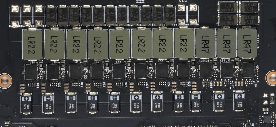
So we see here that a measurement outside on the board with simple measuring resistors can never be done in real time and certainly not accurate enough.
So what’s the point of ICX?
From a marketing point of view, the question is obvious, because you don’t want to give up your cherished unique selling propositions (which really used to be unique), even if it doesn’t make any sense from a technical point of view. Because since Turing, NVIDIA also allows an asymmetrical fan control subject to different factors, which is also based on the values determined in real time for the GPU (including Tjunction), the memory and the voltage converters. This cannot be technically solved any better with a proprietary solution based on board measuring points. On the contrary, you will mait significantly worse in the meantime.
If then a (presumably) faulty board layout causes a MCU to be destroyed (overvoltage?) and already outputs the most absurd values in the drift range, then such a superfluous solution simply has no place on such an expensive board. It’s like an appendix. No one needs him and yet he only flies out when he causes problems. Reason enough for EVGA to bury this relic. There are now enough sensor values that you could display in the EVGA software and do justice to the RGB kiddie universe. From a technical point of view, nobody really needs all that anymore.
And in the end, it’s like a car: what’s not in it in the first place can’t break down!


21 Antworten
Kommentar
Lade neue Kommentare
Veteran
Veteran
Urgestein
Urgestein
Urgestein
Mitglied
Mitglied
Veteran
Veteran
1
Urgestein
Veteran
Veteran
Mitglied
Urgestein
Urgestein
Veteran
Urgestein
Urgestein
Alle Kommentare lesen unter igor´sLAB Community →