


PowerColor’s new factory certainly has the charm of a somewhat unusual test environment, because the one production line installed so far looks more like a small series and test run area. So it’s more like the highly qualified Maggi cooking studio for graphics cards, only with PowerColor out of a can and colorful pixels instead of stock cubes. It all seems more like playground and test track for exploring the best methods and testing the latest equipment. But this is not (yet) normal mass production. Nevertheless, there’s a lot to learn and marvel at, if you get the circumstances right.
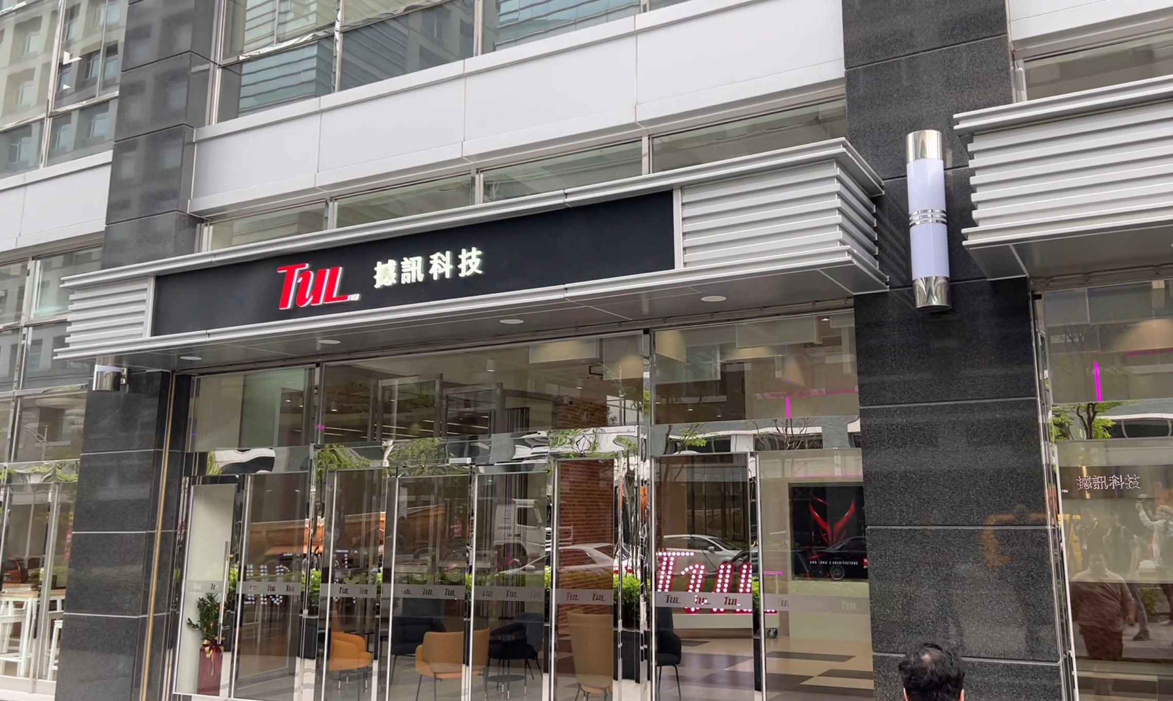
PowerColor is a renowned manufacturer of graphics cards and a brand that is highly regarded by gamers and PC lovers, also because of its comparatively low prices. The company has made a name for itself especially with its AMD Radeon graphics cards, which are sold under various distinctive sub-brands like Red Devil, Hellhound and Fighter. But PowerColor’s portfolio is broader than one might initially think. In addition to graphics cards for gaming PCs and MXM modules (graphics cards for notebooks), the company also produces FPGA cards, motherboards, external graphics card enclosures, video signal control devices, Thunderbolt and USB docking stations, and M.2 NVMe SSDs. However, all of these products are not sold exclusively under the PowerColor brand. TUL, PowerColor’s parent company, also operates other brands and engages in ODM/OEM activities. The production capacity in the new facility is up to 2,400 PCBA (PCB assemblies) per day and the ability to produce up to 1,440 finished high-end graphics cards such as the RX 6900 or 7900 XTX.
The manufacturing process in this facility is elaborate and multi-layered, with a high degree of quality control at every stage. This begins with the quality inspection of the various electronic and non-electronic components that make up a graphics card. On the assembly line, the components are placed on the bare circuit boards. In final production, the finished circuit boards are connected to the non-electronic components (such as heat sinks and back plates) before being packaged.
The first step on the assembly line is the precise application of solder paste to all solder joints on the PCB. This is followed by the placement of components onto the PCBs. The smallest SMDs are placed first, followed by moderately sized components (such as larger capacitors, inductors, connectors, etc.), and finally the largest components, which are fed to the machine in trays (such as the GPU ASIC). After assembly, the PCB passes through a convection reflow oven where specific areas of the PCB are exposed to specific temperatures. This causes the solder to melt and cool, and the component is soldered to the PCB. Following this, the PCB is inspected using an X-ray scanner to ensure that all components are soldered correctly.
However, I have shortened these videos and some sections or omitted them altogether. We had already written several times in detail about these operating procedures, so that I have selected here only once the parts, which fit also to the current topic of the production problems occurred. But before we are allowed into the actual production, we all get a good blow-through. Of course, only after we had put on nice full-body pelts. Including hairnet (how silly on me). So let’s get into the videos together at this point.
After the air shower, I’ll just jump ahead to the station where the backplate of such a Radeon RX 7900XTX is bolted to the board from the top. Because that’s exactly what we’re most interested in with respect to the previous articles. The videos are all in the original sound, because I deliberately refrained from a subsequent voice-over.
And now, of course, it gets really interesting, because PowerColor has experimented with various application methods and quite obviously also changed the paste. The current method is practical, because it avoids too thick, monolithic layers. The compromise between the distance between the surfaces and the thickness of the mask (= later thickness of the layer) results in a homogeneous, sufficiently thin layer between the GPU and heatsink later in total under the contact pressure of the cooler.
On the next page, we will also learn firsthand how exactly this should and can happen with the support of the cards affected by the hotspot problem, because some facet was not even known like that yet. This is new and exclusive today. So please scroll on!


36 Antworten
Kommentar
Lade neue Kommentare
Veteran
1
Veteran
1
Urgestein
Urgestein
Urgestein
Mitglied
1
Urgestein
Veteran
Urgestein
Urgestein
Veteran
Urgestein
Veteran
Urgestein
Veteran
Urgestein
Alle Kommentare lesen unter igor´sLAB Community →