Of course I can’t test 14 motherboards, because on the one hand I have to get the samples from the shops or even buy them myself and on the other hand I lack the time and resources to do so with the necessary care and constant verification measurements. My thanks go again to X-Hardware, a local dealer from Chemnitz, who (certainly not without his own interest) lets me test motherboards from time to time.
Therefore I will limit myself to three motherboards for this article, of which I know after the short test a larger selection of motherboards that they will really cover all scenarios sufficiently. At the end of the selection, an Asus Prime X570-P, an ASRock X570 Pro 4 and an MSI X570-A Pro, all with the latest BIOS, i.e. the respective entry-level models of the three manufacturers, are examples of the selection. In addition to that I measured an A320M S2H V2 for a good reason – not only to sound out the limit downwards and to round it off a bit, but also because the chipset acted quite fast. In conclusion even more.
But I have to make a preliminary remark, because in this article I refer very consciously to Allcore, i.e. the clock rate that is possible with all cores at the same time. The current discussions about the maximum possible boost clock on one or two cores are not or only indirectly affected by this, because such things are based on firmware optimization, while today’s problems also and above all concern design and component assembly.
Sensor values beyond any logic
Why I don’t want to and can’t do the actual motherboard test is quickly explained. One can certainly compare the performance or simply point the infrared camera at the voltage regulators, but this hardly brings an informative added value, if one does not go into the sometimes considerable differences that occur when measuring directly at the hardware and indirectly reading out the sensors. Therefore I will start with a table of what I have measured or read out. Exactly this is however provided with so many question marks that it could become bad. For the sensor values I used HWInfo64 6.10 and compared it with other programs like Aida64. The readout values were always identical (with errors).
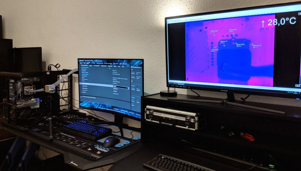
The actual setup is relatively simple. With the Alphacool Eisbaer Extreme a normal All-in-One compact water cooling is used and not the chiller. The room temperature is constant, so that I can also check the CPU temperature behaviour between 30 and 80 °C. With the exception of the motherboards, the components are always the same and also the general conditions are largely the same within the scope of my possibilities. With the Ryzen 5 3600X, I also use a 95-watt CPU that can also be used very precisely as a heat dispenser in this TDP range. With one exception, but I’ll get right to that.
Let’s first take a look at the table showing the boards in their default state (BIOS defaults) and understand why one shouldn’t and shouldn’t limit oneself to pure readout values. The values are the average of 15 minutes full load with Prime 95. I actively cooled the A320 board in the VRM area, because otherwise the safe and stable operation would not have been possible. I measure the passive GT 1030 at the slot and subtract the measured value from the 24-pin connector.
| Values | Asus Prime X570-P |
MSI X570-A Pro |
ASRock X570 Pro 4 |
Gigabyte A320M S2H V2 |
| 12 Volt EPS (Measuring) | 107.8 W | 118,9 W | 122.4 W | 114.7 W |
| 12 Volt 24-Pin (Measuring) | 5.2 W | 6.4 W | 4,9 W | 5.8 W |
| Package Power (Sensor) | 105.8 W | 119.2 W | 53.6 W | 97.1 W |
| CPU-Power (CPU Cores, Calculation) | 91.5 W |
88.2 W |
92,2 W |
89.7 W |
| CPU-Power (Sensor) | 59.9 W | 87.4 W |
38.1 W |
77.2 W |
| SoC-Power (Sensor) | 14,1 W* | 7.71 W | 4,3 W | 8.9 W |
| CPU + SOC (Sensor) | 73.9 W | 95.1 W | 42.4 W | 86.2 W |
| CPU + SOC (Calculation) | 105.6 W* | 94,7 W | 96,3 W |
98.3 W |
| Core Clock (Average) |
4076 MHz |
4061 MHz |
4073 MHz |
4061 MHz |
The Asus motherboard is the only one equipped with DrMOS. The Power Stages (SiC639 from Vishay Siliconix) are not yet the upper end of the food chain, but for this price point they are very praiseworthy. This can also be seen in the very high efficiency of the voltage converters, which in practice is probably only just under 95 percent in the CPU area. The other boards, which are all equipped with single MOSFETs, perform much worse and are only in the lower 80 percent range.
The consequences can be calculated quite easily, because the most efficient board is not only the fastest, but also the coolest. But if we then look at the respective sensor values of the boards, we also notice that what the motherboard calculates often enough has to be completely wrong, because the values are simply not plausible. The laudable exception is the MSI board, which is almost always in the range of plausible values, followed by the cheap gigabyte A320M, which is a bit off, but still remains acceptable. The biggest deviations are provided by the ASRock board, whose sensor values are completely unusable. I’ll have to make some further remarks about this board later, because the BIOS is simply faulty to questionable.
Inductor DCR as first attempt at explanation
I don’t want to chew anyone’s ear off for hours, but I have to put some theory into it. The information about the flowing currents is either obtained directly from the MOSFETs (drain measurement), then one speaks of a MOSFET DCR (Direct Current Resistance). Current Smart Power Stages (SPS) offer this return value as IMON even in very small intervals and very exactly. However, for cost reasons, none of the boards has the necessary combination of SPS and suitable PWM controller built in, so that all four motherboards have to rely on the so-called Inductor DCR.
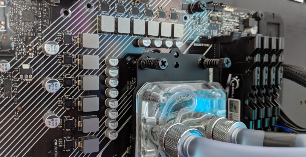
DCR (Direct Current Resistance) is the basis for calculating temperatures and currents. But how does the controller know exactly which currents flow in which control loop? The voltages are known, but due to the extremely high currents, you can’t simply rely on shunts and the resulting voltage drop for the current flow. This is where the so-called Inductor DCR comes into play, i.e. a current measurement via the inductive resistance of the respective filter coils in the output area. However, the accuracy of this very favorable solution is significantly lower and is also strongly influenced by fluctuations in the component quality. Tolerances that are too large can quickly tilt the complete balance.
In addition, these results are rather estimates and calculations, but not direct measurements in the conventional sense with a definable tolerance range. What can be classified as quite reliable or plausible in the values of the above table are my measurements on the motherboard connections and the return value of the CPU over the individual cores and their power requirements. This information turned out to be reliable. Since the SoC value, which concerns e.g. the I/O controller, the memory controller and other smaller loads, can be put at 7 to 10 watts (depending on the model, information from a board partner), there are at least some reliable values left which can be used as a basis. For example, the 14 watts that Asus outputs here are rather unlikely, otherwise the voltage converters would already be almost in the 100% range in terms of efficiency. Therefore I marked the value in the table with a *.
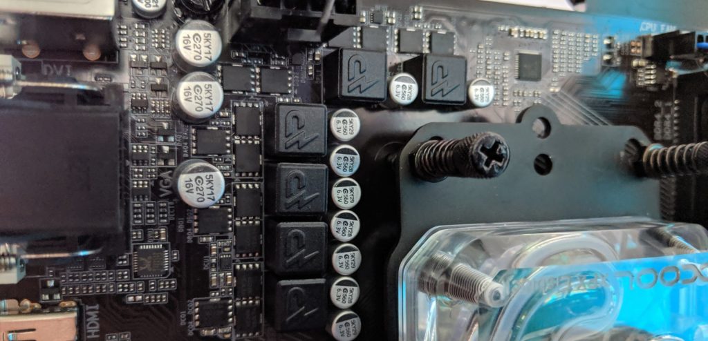
Finally, if one considers the maximum clock rates (all cores averaged over 15 minutes) with what I have listed in the table as CPU + SoC (calculation), then this wattage corresponds quite well with the clock rate achieved. At the end, the boards are more or less the same at the clock rate, if you include the measurement tolerances, but differ in the real power consumption. Before we continue now, I would like to insert an important note to be able to classify the following emotionlessly better:
All boards with VRM coolers had no problems with higher loads, even if the voltage regulator losses were higher with one or the other board. If I later measure the boards without heat sinks, this is only for demonstration purposes and not because one of the boards would have been unsuitable for its task. The choice of components is always subject to cost constraints, so that you have to accept some compromises as long as the functionality and possible durability are not demonstrably affected.
Just a quick look at the test system and you’re ready to go:
| Testsysteme und Messräume | |
|---|---|
| Hardware: |
AMD Ryzen 5 3600X 2x 8GB Trident DDR4 3600 1x 1 TB OCZ SSD 1x Seagate FastSSD Portable USB-C Seasonic Prime 1200 Watt Titanium |
| Cooling: |
Alphacool Eisblock XPX Alphacool Eisbaer Extreme |
| Benchtable: |
Raijintek Paean (open, no glass) |
| Monitor: | Eizo EV3237-BK |
| Power Consumption: |
Non-contact direct current measurement on the PCIe-Slot (Riser-Card) Non-contact direct current measurement at the external PCIe power connectors Direct voltage measurement at the respective connectors and at the power supply unit 2x Rohde & Schwarz HMO 3054, 500 MHz Multichannel Oscilloscope 4x Rohde & Schwarz HZO50, Current Clamps 4x Rohde & Schwarz HZ355, Probes 1x Rohde & Schwarz HMC 8012, Digitalmultimeter |
| Infrared: |
1x Optris PI640, 2x Xi400 Thermal Imager Pix Connect Software |
| OS: | Windows 10 Pro (1903, all Updates), latest drivers and firmware |






Kommentieren