


Power consumption and temperatures
In idle mode, the power consumption is around 750 to 780 mW, which I can measure directly at the adapter. In normal mode (workstation workloads, gaming), the entire SSD consumes a bit under 4 watts, which already wants to be cooled. The maximum of 6.05 watts in peak (typically 5.8 to 5.9 watts) during continuous copying is something that can’t be done without proper cooling. Thermal throttling is a bit over 80 °C, which then slows the SSD down to well below 1 GB/s until it cools down. The M.2 slot cooler is basically sufficient, but it could certainly be much cooler with a good cooling block and some air movement.
Controller and NAND memory
Most consumer NVMe controllers rely on Cortex-R cores from ARM. These are special processor cores that are specialized for real-time applications such as latency-sensitive I/O. The SK hynix Aries SSD controller, manufactured in 12 nm, is larger than its direct predecessor and the larger surface area is very conducive to heat dissipation. Unfortunately, not much is known about the controller, but it supports both trim and S.M.A.R.T. for the 8-channel controller. Like other controllers, it uses Active State Power Management (ASPM), Autonomous Power State Transition (APST) and L1.2 ultra-low power state. Thermal throttling is implemented but the large surface area of 17 x 17 mm also allows you to do without an integrated nickel heat sink, unlike many other models. Unfortunately, you don’t get much more data, which is a pity.
The 1 TB model uses 1 GB LPDDR4 from SK hynix, and the 2 TB model would have 2 GB. The DRAM on the SSDs is most often used for metadata, especially mapping and addressing to translate between physical and logical data stores. DRAM already has inherently much lower latency than NAND, making it particularly useful for many small and random I/O operations. This is especially true for writes, since they require updating the look-up table (LUT). The DRAM stores the currently current or most frequently used data accesses.
SK hynix uses its own 176-layer TLC flash in this drive. However, the flash density cannot be directly compared with those of the competitors, but it could well be on the level of BiCS6 or Micron’s current TLC memory. 8 channels with 1600 MT/s each. Unfortunately, the documentation here is also sparser than my head hair. Again, too bad.

What does dynamic pSLC cache actually mean?
Now we come to a more technical detail that most people might not be aware of to the full extent. Much has already been written about pSLC cache, so there is no need to go through it again in detail, at most as a small refresher. Here we go…
To increase the write speed, the so-called “pseudo-SLC cache” (pSLC) is often used in consumer products, although it can now also be found in various industrial solutions. For this purpose, part of the NAND capacity is configured as SLC memory, in which only one bit per cell is stored. Accordingly, this memory can be written and read very quickly. Since it is not dedicated, i.e. not a real SLC memory, it is called pseudo SLC. Such a cache can be used for all memory types that store several bits per flash cell, i.e. three bits as here with TLC. The pSLC cache also uses a significantly higher voltage for the one bit, which provides some security and is therefore better than Fast Page.
The use of pSLC cache offers a speed advantage, especially when the storage medium is not busy with read or write accesses between writing larger amounts of data. These idle times are used by the storage medium to move data from the cache to the TLC area.
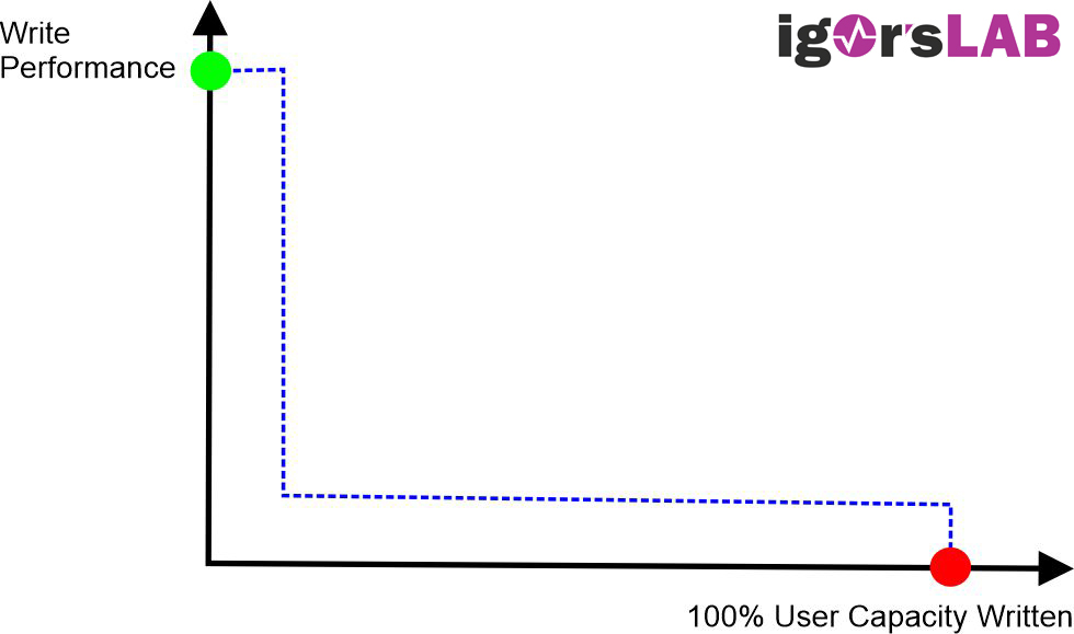
But everyone knows the disadvantages of the pSLC. When the fast pSLC cache is full, the speed drops significantly because further write accesses to the storage medium must first free the pSLC by moving older data from the cache to the TLC memory.
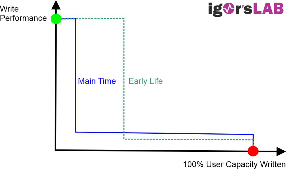
But what is hidden behind “dynamic pSLC cache”? Dynamic pSLC cache has now also found its way into industrial storage solutions, but only with very hard restrictions. In contrast to the static pSLC cache, up to 100% of the NAND flash is used dynamically as pSLC cache, depending on how full the storage medium is. The cache can thus comprise up to 1/3 of the total memory size
However, the writing speed of the storage medium depends not only on the amount of data that is written without interruption, but also on the fill level of the memory. And this is exactly what makes the write speed in the life cycle difficult to predict.
NAND flash manufacturers do not recommend dynamically changing the configuration of flash blocks as pSLC or TLC memory for reliability reasons, but in the consumer sector, where the temperature windows are not so important, people are more relaxed about it.
All manufacturers of dynamic NAND storage media media, including SK hynix, permanently switch back to TLC mode after a specified maximum number of program and erase cycles. Before that, the storage medium achieves the best values especially in short write processes that do not require the entire capacity. After a certain amount of use, however, the medium slows down permanently, and this should never be ignored. Phison’s E18 handles dynamically changing the configuration of flash blocks quite well, but it can’t outsmart physics either.
When you will reach the end of the great cache performance is such a thing with imponderables here. After about 210 GB in one piece, the glory was over for the time being and at a bit more than 85% of the capacity, you are only on a mediocre SATA level. In practice, this will hardly be possible, but it is better not to write in full in one piece and perhaps more than once.


9 Antworten
Kommentar
Lade neue Kommentare
Mitglied
Veteran
Urgestein
1
Mitglied
1
Neuling
Mitglied
Veteran
Alle Kommentare lesen unter igor´sLAB Community →