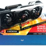
The launch of the Radeon RX 6750XT is a week ago and the prices are falling. It’s about time again to test a board partner card with the Sapphire Radeon RX 6750 XT Nitro+ 12 GB, which is either more frugal or thirstier than the older RX 6700XT and can thus be faster or a bit slower. Either, or – by the way, the two generations will never exactly meet in the test, and that’s a good thing. With a current street price of 648 Euros and a slight downward trend, the card hardly leaves room to breathe for Intel’s upcoming “flagship” and we can already see where the journey will probably go with Team Blue’s disk launch. In this regard, I also refer to the section with power consumption and efficiency in this article, because we also want to see where the journey is still going and which bar Intel will obviously have to break soon (if at all). Because when there are no more major changes in the drivers, it gets boring and the 6650XT has to stand at attention in the blue suit.
But back to Sapphire and AMD, because Intel is currently still blue curd in the shop window. With the (Attention! Officially prescribed name according to AMD’s nomenclature) “NITRO+ AMD Radeon™ RX 6750 XT Gaming Graphics Card with 12GB GDDR6, AMD RDNA™ 2”, which I will call Sapphire RX 6750 XT Nitro+ again in the article for the sake of simplicity (as otherwise the charts and legends would explode) here lies a thoroughly interesting RDNA2 specimen that you have to listen twice (or three times) to hear. Speaking of designation and charts, all tested cards are board partner models, to be fair. Where the Nitro+ is not listed as Perf or Silent in the chart labels, the AMD cards are MSI’s factory overclocked Gaming X series board partner cards, and the NVIDIA cards are the SUPRIM X series. Unfortunately, I have to take this step, because otherwise the names, which are as long as a horse, will become almost as long as the much more interesting bars.
This graphics card, like all RX 6000 models, can handle the new AV1 video codec, they also support DirectX 12 Ultimate for the first time and thus DirectX Raytracing (DXR). With AMD FidelityFX, they also offer a feature that should also give developers more leeway when selecting effects. Variable Rate Shading (VRS) is also included, which can save an immense amount of computing power by smartly reducing the display quality of image areas that are not in the player’s eye anyway. So much for the feature set of all new Radeon cards.
Optics and haptics
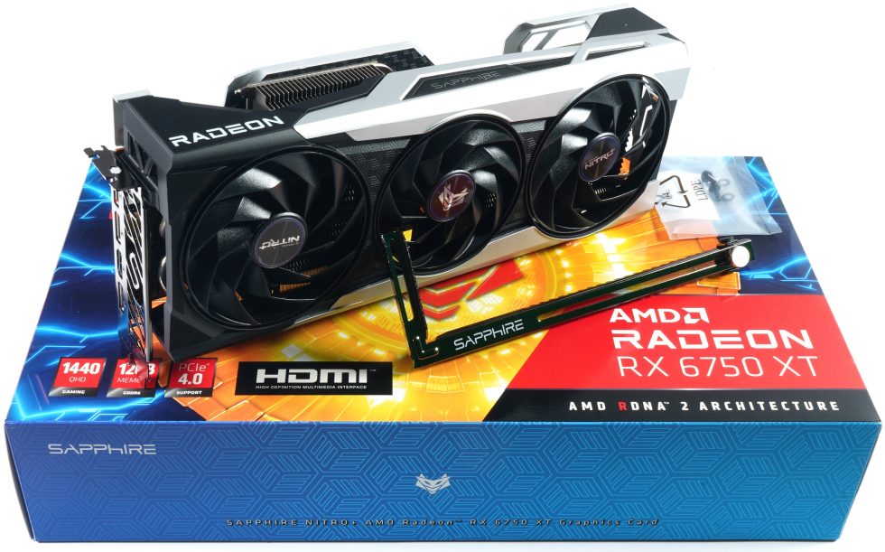
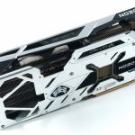
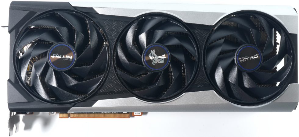
The Sapphire RX 6750 XT Nitro+ weighs 1161 grams and is thus almost a flyweight. Nevertheless, a graphics card holder is included for free. It is thus also considerably lighter than the MSI card from the launch article and with its full 31.5 cm it is also quite long. In addition, there is the usual 12.5 cm installation height from the PEG and a thickness of 5.8 cm, with a backplate and the PCB adding a total of five more millimeters.
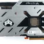
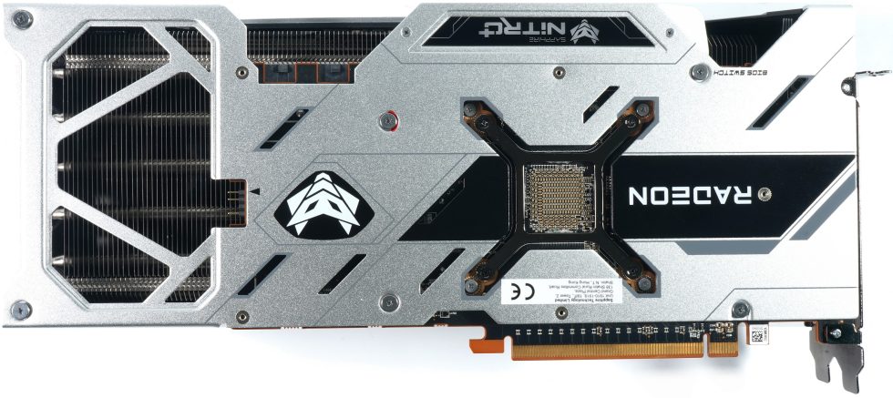
The two-tone body (black and gray metallic) is made of ABS, the Sapphire lettering on the top and the Nitro+ light band on the back (backplate) are LED illuminated. In contrast to the front, everything at the rear is nicely finished in light metal instead of plastic, which has a lot of haptic appeal.
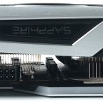
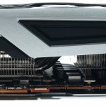
The graphic brick including illumination is supplied via two standard 8-pin sockets, so everything is as known and used from the Radeon RX 6700XT Nitro+. We can also see the vertical alignment of the cooling fins and the board reinforcement in the form of a backplate and the separate RAM cooler here in the picture. But more about that in a moment in the teardown.
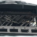
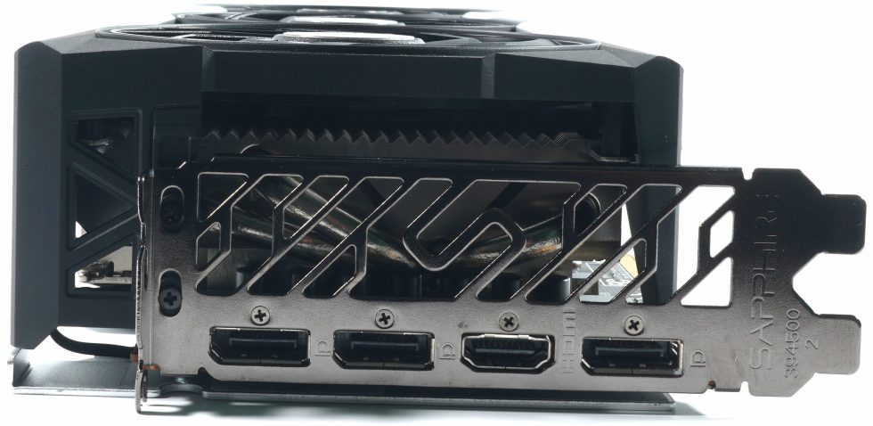
The slot bezel is closed, carries 1x HDMI 2.1 and three current DP ports. However, the USB Type C port is missing. More about the construction, the cooler and the assembly can be found on the next page in the teardown.
Technology
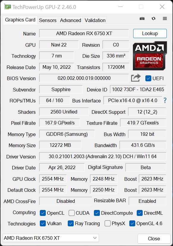
With the 40 compute units (CU), the card has a total of 2560 shaders and is thus virtually “half” a Radeon RX 6950XT. While the base clock is specified at 2495 MHz, the boost clock is 2600 MHz in the Silent BIOS and 2623 MHz in the Performance BIOS, which is also achieved. Card relies on 12 GB GDDR6 with 18 Gbps, which is made up of 6 modules of 2 GB each. This includes the 192-bit memory interface and the 96 MB Infinity Cache, which should solve the bandwidth problem. The card thus fortunately has a switchable dual BIOS, which is nice. When the BIOS DIP switch is set to the left, a switchover can be solved seamlessly and directly via software on-the-fly with Sapphire’s TriXX software.
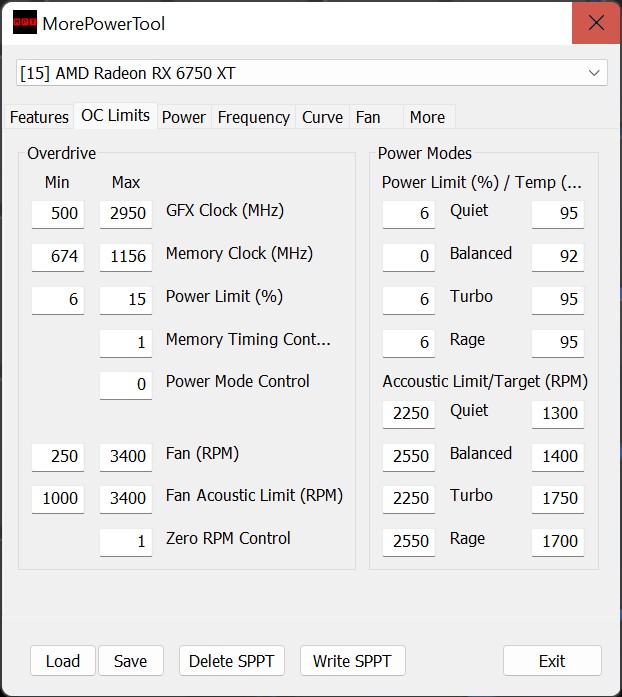
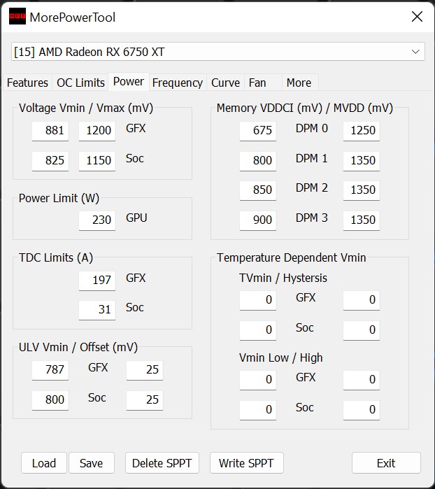
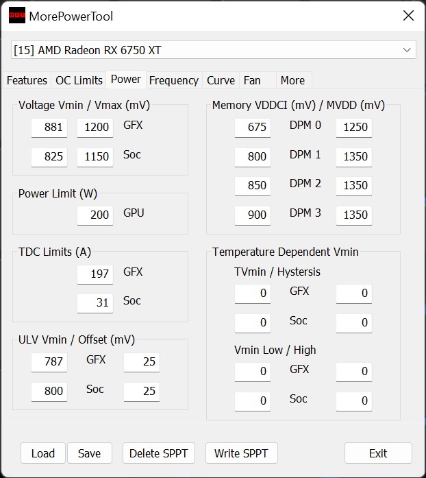
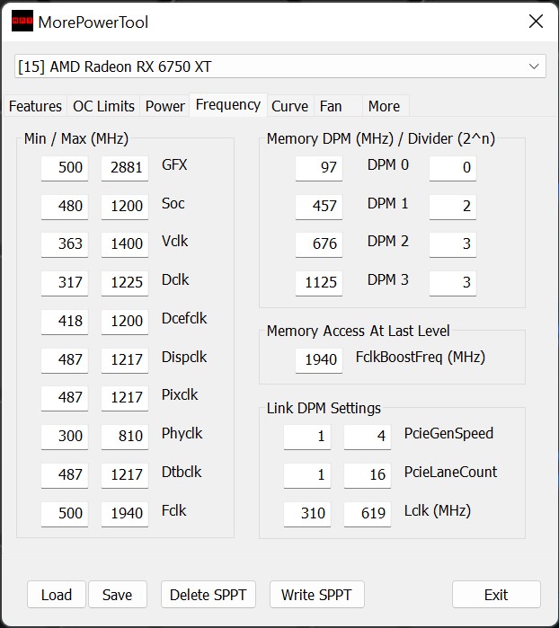
Other data is different in the BIOS, for example the TGP, i.e. the maximum power for GPU, SoC and memory. The performance version offers up to 230 watts TGP instead of 200. The details show the stored values from the MorePowerTool (left respectively the performance BIOS, right the silent BIOS)
Raytracing / DXR
At the latest since the presentation of the new Radeon cards, it is clear that AMD will also support ray tracing. Here, NVIDIA takes a different path and implements a so-called “ray accelerator” per compute unit (CU). Since the Radeon RX 6800 has a total of 72 CUs, this also results in 72 such accelerators for the Radeon RX 6800XT, while the smaller Radeon RX 6800 still has 60. A GeForce RTX 3080 has 68 RT cores, which is nominally less for now. When comparing the smaller cards, the score is 62 for the RX 6800 and 46 for the GeForce RTX 3070. However, RT cores are organized differently and we will have to wait and see what quantity can do against specialization here. In the end, it is an apples and oranges comparison.
But what has AMD come up with here? Each of these accelerators is first capable of simultaneously calculating up to 4 beam/box intersections or a single beam/triangle intersection per cycle. In this way, the intersection points of the rays with the scene geometry are calculated (analogous to the bounding volume hierarchy), first pre-sorted and then this information is returned to the shaders for further processing within the scene or the final shading result is output. However, NVIDIA’s RT cores seem to be much more complex, as I already explained in detail during the Turing launch. What counts is the result alone, and that’s exactly what we have suitable benchmarks for.
Smart Access Memory (SAM)
AMD already showed SAM, i.e. Smart Access Memory, at the presentation of the new Radeon cards – a feature that I also enabled today in addition to the normal benchmarks, which also makes a direct comparison possible. But actually SAM is not Neuers, just verbally more nicely packaged. This is nothing more than the clever handling of the Base Address Register (BAR), and it is exactly this support that must be activated in the substructure. Resizable PCI bars (see also PCI SIG from 4/24/2008) have played an important role in modern AMD graphics hardware for quite some time, since the actual PCI BARs are normally only limited to 256 MB, while the new Radeon graphics cards now offer up to 16 GB VRAM.
The consequence is that only a fraction of the VRAM is directly accessible for the CPU, which requires a whole series of workarounds in the so-called driver stack without SAM. Of course, this always costs performance and should therefore be avoided. AMD thus starts exactly there with SAM. This is not new, but it has to be implemented cleanly in the UEFI and also activated later. This is only possible when the system is running in UEFI mode and CSM/Legacy is disabled.
CSM stands for the Compatibility Support Module. The Compatibility Support Module exists exclusively under UEFI and it ensures that older hardware and software also works with UEFI. The CSM is always helpful when not all hardware components are compatible with UEFI. Some older operating systems as well as the 32-bit versions of Windows also cannot be installed on UEFI hardware. However, exactly this compatibility setting often prevents the clean Windows variant needed for the new AMD components during installation.
Test system and evaluation software
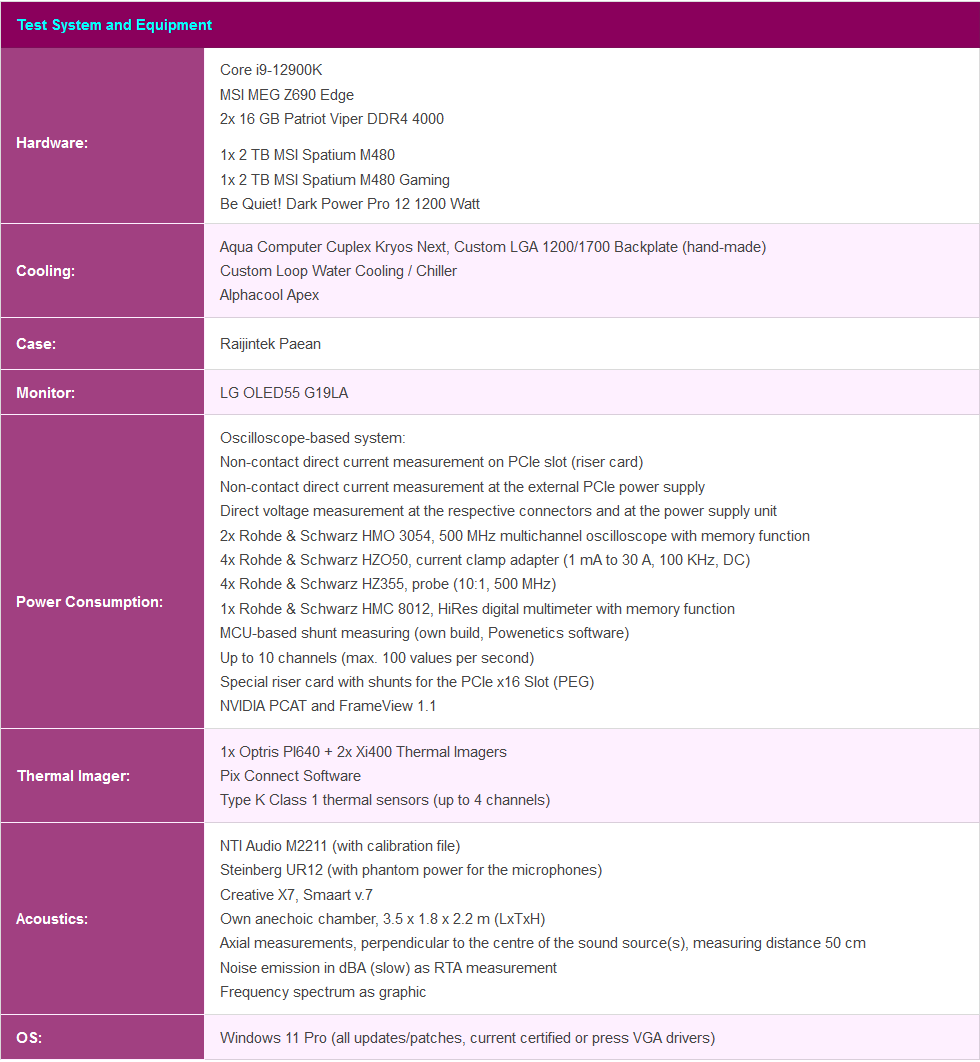
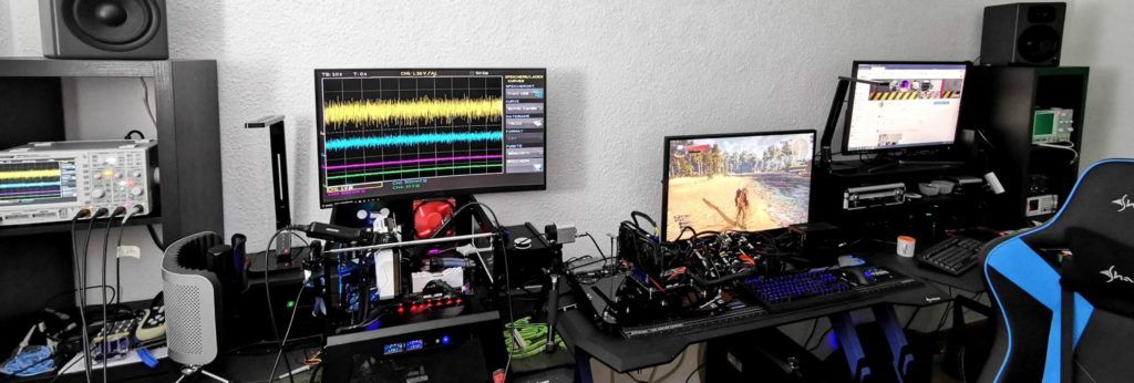
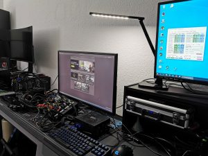
The benchmark system is new and is no longer in the lab, but in the editorial room again. For direct logging during all games and applications, I use NVIDIA’s PCAD and my own development with Powenetics’ software, which increases the comfort immensely. The measurement of power consumption and other things continues to be carried out in the air-conditioned laboratory on a redundant test system that is identical in every detail, but then using high-resolution oscillograph technology..
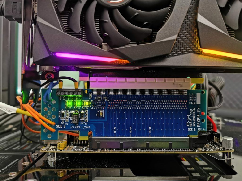
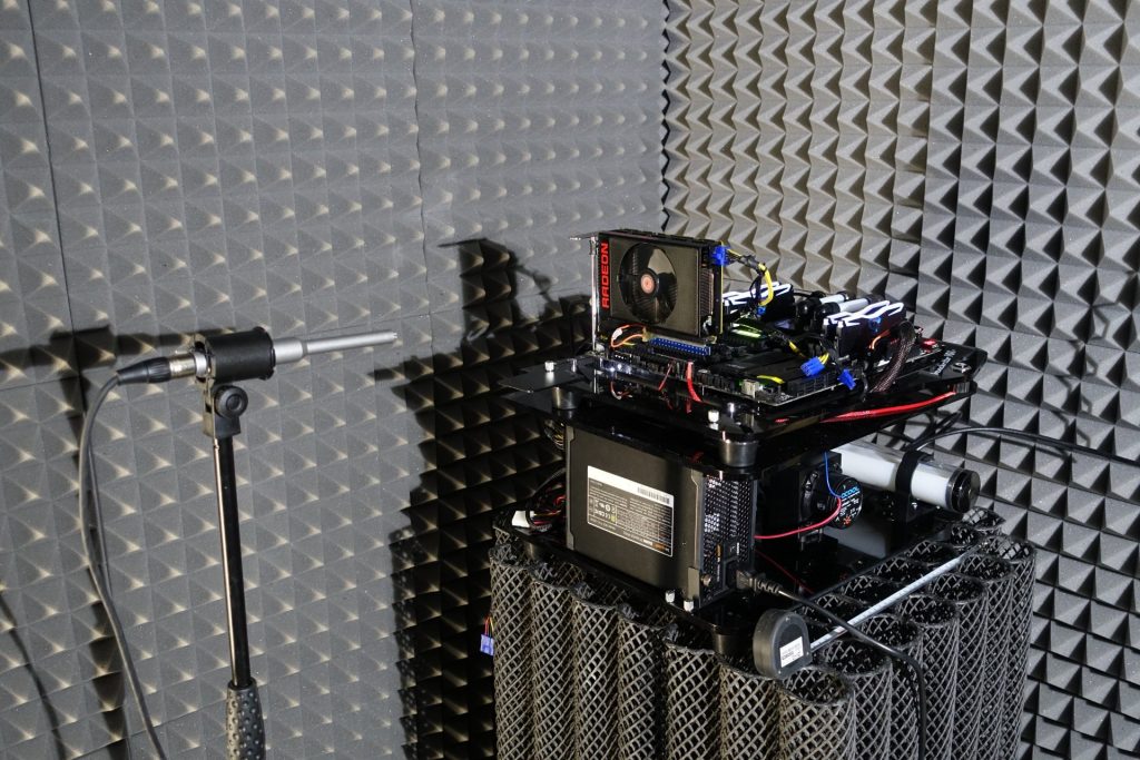
…and the self-created MCU-based measurement setup for motherboards graphics cards (pictures below), where at the end in the air-conditioned room also the thermographic infrared images are created with a high-resolution industrial camera. The audio measurements are done outside in my Chamber (room within a room).
I have also summarized the individual components of the test system in a table:
- 1 - Introduction, Unboxing, Technical Details
- 2 - Teardown: PCB, Voltage Converters and Cooler
- 3 - Gaming Performance
- 4 - Gaming Power Consumption and Efficiency
- 5 - Power Consumption, Load Peaks and PSU Recommendation
- 6 - Temperatures and Clock Rates
- 7 - Fan Curves and Noise
- 8 - Summary and Conclusion
















35 Antworten
Kommentar
Lade neue Kommentare
Veteran
Veteran
Mitglied
1
Veteran
Veteran
Urgestein
Urgestein
Urgestein
Veteran
Mitglied
Veteran
Mitglied
Mitglied
1
Veteran
Veteran
Alle Kommentare lesen unter igor´sLAB Community →