


Phison PS5019-E19T
The package of the relatively new Phison PS5019-E19T controller already attracts attention with its small dimensions. It measures a whole 7 × 11 mm and already suggests a clearly fancy, inner simplification. The casing of the well-known Phison PS5016-E16, for example, is even almost three times larger, although the same 28 nm node from TSMC process is used for manufacturing. The reasons for the shrinkage cure are also quickly explained.
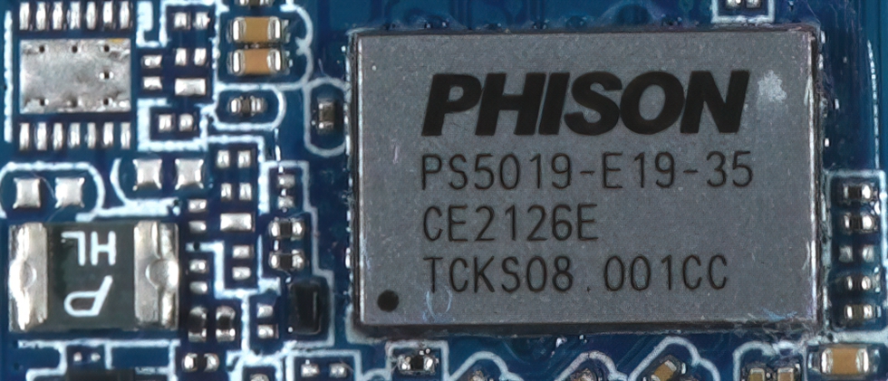
Thus, the Phison PS5019-E19T is based on a single-core rather than dual-core ARM Cortex R5 processor. For this, the number of possible channels for connecting the flash memory is reduced to four instead of eight, which also somewhat limits the use of certain modules (number, size). By the way, the DRAM interface is also missing, but I already wrote something about the unbuffered operation on the first page. The Phison PS5019-E19T is thus a truly extreme (but purposeful) stripped-down controller designed for building low-cost, unbuffered SSDs with PCIe 4.0 support. And it is also more frugal with a power consumption of well under 4 watts, which makes it significantly cooler than the E16 or E12 models.
Abandonment of the DRAM buffer
Buffer-free products like the Samsung 980 or the WD Blue SN550 have been on the market for months and show that it is possible to do without DRAM with certain restrictions. However, the PCIe 4.0 bus with increased bandwidth, which should theoretically let the SSD controller work more efficiently with the PC’s RAM, does not always help. This is because it is also important to remember that the lack of a dedicated DRAM forces the controller to use only HMB (Host Memory Buffer) technology to work with the address translation table.
Unfortunately, this also means that the drive will fork a certain part of the PC’s memory (up to 64 MB) for its own purposes during operation in order to buffer calls to the flash memory array. As a result, the SSD’s speed decreases like an avalanche under high load in certain scenarios, which especially affects the read process very much. If you have to process more than 32 GB of information in one go, it can get quite tight.
The drop in random reading can be more than half, or it can be mitigated or circumvented by tricks in the controller. However, it is a fact that an unbuffered SSD is rather poorly suited for many intensive workloads. You have to scrutinize yourself, the area of application and the applications used. For that, I’ll have a detailed workstation test with the comparison to a “conventional” PCIe 4.0 SSD with DRAM later.
Micron’s 176-layer TLC 3D NAND (codename B47R)
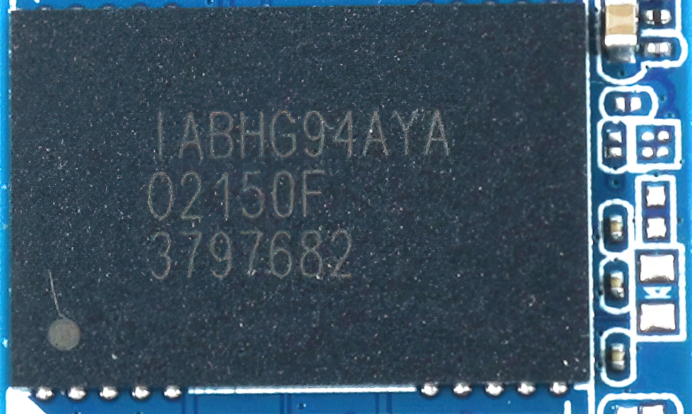
The Phison PS5019-E19T just described is compatible with a wide range of flash memory variants and supports modern NAND chips with 1200 MHz interface. And because it’s so nicely compatible, if you’re a low-cost NVMe SSD vendor, you can also use Micron’s latest 176-layer TLC 3D NAND (codenamed B47R) with it. For example, the MSI Spatium M450 I tested contains two IABHG94AYA chips, each with eight 512-gigabit TLC 3D NAND blocks inside.
By the way, Micron’s still quite new 176-layer flash is the first real in-house development by Micron after the separation from Intel. This memory is also very different in its internal structure from the products of all other manufacturers. The cell structure of the Micron NAND relies on replacement gate, which ends up being a cross between floating gate and charge trap technologies. Micron replaced the polysilicon in the gate material with metal in this NAND and switched to a different process for etching the vertical cylindrical channel, resulting in an increased diameter.
In addition, a non-conductive layer of silicon nitride has been introduced into the structure of the micron memory, in which data can be stored. This layer also reduces quite effectively the mutual interference of the cells in such a vertical stack. Of course, we can go into a little more detail. The next figure shows a chip looking at the metal top, a chip looking at the CMOS circuits (CuA) and the markings of the B47R chip. Compared to the older B37R TLC die, the chip size has been reduced by a whopping 25% due to the higher cell density, larger number of 3D NAND cells and effective scaling of the design. The B47R is now Micron’s second generation CTF structure after the B37R.
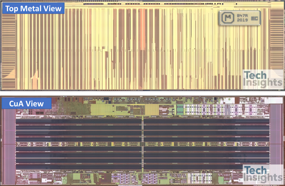
The height of the NAND cell array (for comparison: the height from the selector on the source side to the BL) is now more than 11 µm. The total number of gates, including selectors (STs) and dummy word lines (DWLs) per vertical NAND strand is 195, or 195T, which is the highest number ever achieved in 3D NAND. They rely on double-stack architecture, the replacement gate process, charger trap nitride (CTN) and CMOS-under-array (CuA) techniques. The bit density reaches 10.273 Gb/mm2 for the 512Gb TLC die.
Thus, in the end, it was possible to achieve a number of positive effects, because it was possible to increase the speed of the programming cells, increase their stability, reduce power consumption and at the same time also improve the reliability of data storage. Ultimately, Micron’s 176-layer TLC-3D NAND thus takes the next step in 3D flash technology in general. And in terms of performance, Micron claims that the new memory has reduced read and write latency by about 35% compared to the previous generation 96-layer memory. Well…


7 Antworten
Kommentar
Lade neue Kommentare
Mitglied
Veteran
Mitglied
Urgestein
Veteran
1
Neuling
Alle Kommentare lesen unter igor´sLAB Community →