


Yesterday we were allowed to publish the first own pictures of NVIDIA’s upcoming graphics card generation, but we still have to keep quiet about further details up to the performance until the set launch day. Some clarification (certainly also in the sense of NVIDIA) would be urgently necessary. Because the outcry about the huge, heavy cooling solutions after the first unboxing articles and videos was really enormous. All the nastiness about supposed power guzzlers, overtaxed power supplies and load peaks that are said to be higher than Mount Everest would be over long ago if the backgrounds were better communicated.
But where does the rumored high TBP of 600 watts come from and the associated necessity to adequately cool this huge amount of waste heat and to have to buy a new power supply? And why is it now suddenly only 450 watts, as is reported everywhere? The answer is simple, but unfortunately the reason has never been openly communicated. NVIDIA could certainly have saved itself a lot of gloating and ridicule in the process. I’ll have to go a bit further, because I’ve already written a few articles on the topic of power consumption and waste heat.
The real reason for the originally set 600 watt default power limit is Samsung and the very inefficient, old 8 nm node, for which Ada was planned for its part. This is exactly the amount of energy that would have been required to achieve the increases in clock speed needed to boost performance. And because you have to plan graphics cards for the long term and of course get all the parties involved, such as the entire board partners (AIC), on board in advance, the entire key data is of course always the worst-case scenario including all the necessary reserves.
Where the 600 watts of the NVIDIA GeForce “RTX 4090” actually come from – an estimate of GPU and components
If NVIDIA had really had to manufacture the new generation at Samsung in the 8 nm process, this article would of course have been superfluous today. All designs and components were developed to match the 600 watts of power consumption, because the necessary lead time of a few months was needed. Well, and then TSMC came along. The switch from Samsung to TSMC’s much better 4 nm process is the absolute turning point here, including the (positive) consequences that no one could have foreseen.
According to my own sources in Taiwan, the yield of the chips produced is so high that not only the quantity of what can be effectively utilized was higher than expected, but also the quality of the chips. Thus, it was probably possible to reduce the power consumption considerably for the performance target (it is rumored to be around 33 percentage points) and is thus roughly on the level of the (still) current generation.
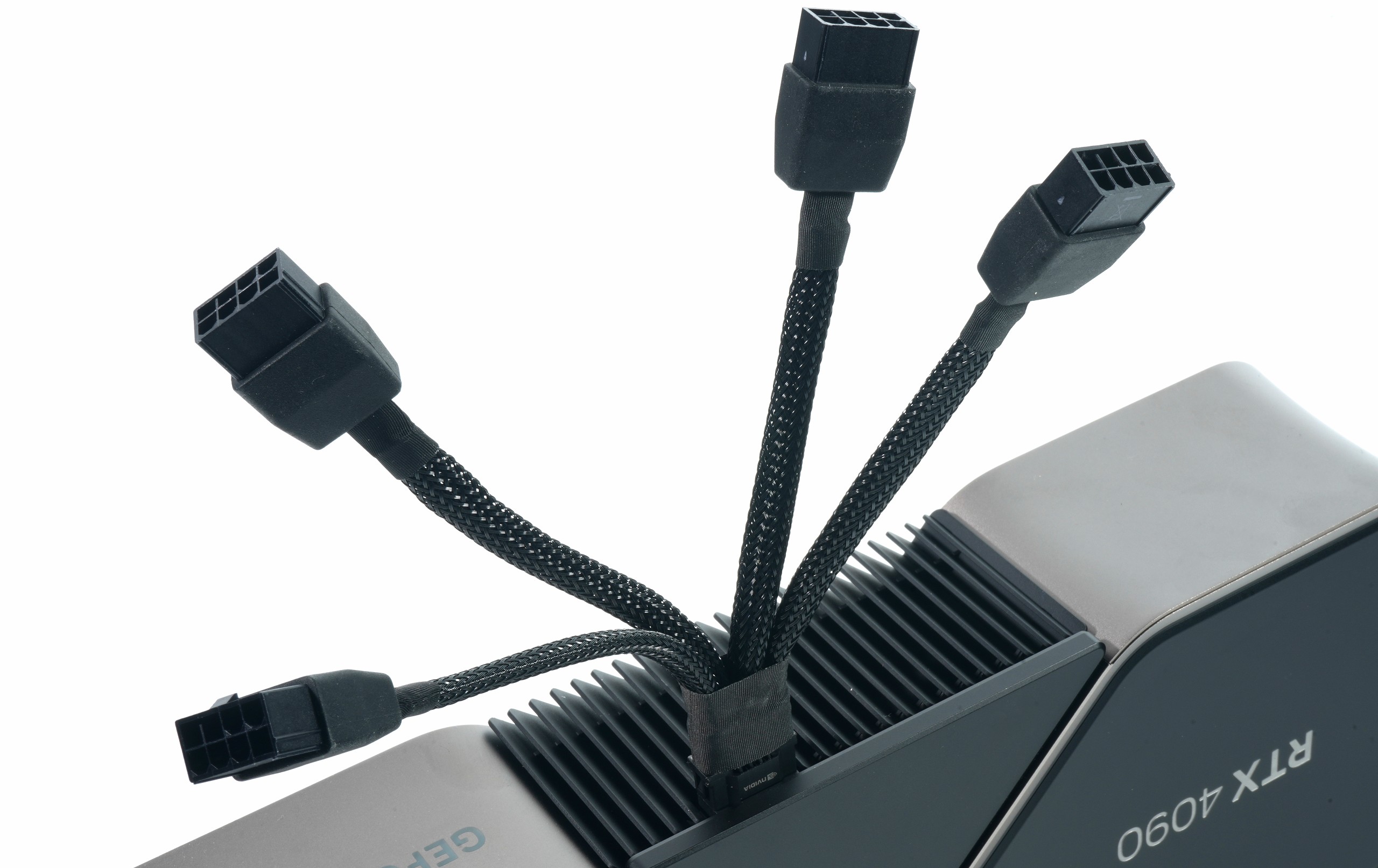
However, based on the Thermal Design Guide distributed to board partners and third-party vendors at the time, all cooling solutions were designed for the truly extremely high 600 watts. I also wrote in an older article that the GeForce RTX 3090 Ti was supposed to be the playground for the new graphics cards and that the pin-compatible GA102 had been bored to 600 watts in the test vehicles via suitable firmware in order to be able to evaluate the electrical and thermal problems meaningfully in advance.
If you ask the responsible developers at AIC today, they would certainly have liked to spare themselves the cooling stunt. Internal tests should also show that the existing cooling solutions for the GeForce RTX 3090 Ti would have been sufficient. However, what is ordered is always delivered, and so we will certainly see many cards whose TBP will once again slightly exceed the new 450 watts that have been rumored. Not because they have to, but because they simply can. There are enough reserves, even for overclocking and as a graphical replacement for the expensive gas heating. However, the voltage limits of the VDDC should be reached very quickly, which should make an increase to values above 500 watts superfluous.
Because the VF curves should also only last up to 450 watts, no matter with which limit a card is sold and the rest is then just pure heating. I can’t give more details here, because there are unfortunately also blocking periods and I only cover the reports of third parties.

In line with this leaked information from the accessories industry and AIC, it seems that they have lowered the power consumption of the upcoming GeForce RTX 4080 16 GB from the initial 420 watts to 340 and later even to 320 watts, and the card could still be faster than expected. So, as AIC, you ordered clothes in XXXL format, which ended up being much too big due to the sudden change of food supplier and the resulting weight loss. But there is a point of no return in industrial processes, so everything is just the way it is now.
As a potential buyer, this can also be seen positively, because it can be assumed that all coolers will work with above-average sovereignty and quietness. However, some board partners are said to complain internally that they would have liked to save the additional costs of more than 10 USD per cooler. If you extrapolate this to the units to be produced, the sums quickly become really huge.
However, the last monolithic jumbo jet’s surge towards efficiency could well claim other prominent victims than just bent motherboards with the corners of their mouths pulled down. The efficiency boost, which is certainly unexpected for some, could probably also throw AMD’s next generation into a bit of a tailspin, since it does not rely on TSMC’s latest node, but on a mixture of older processes for GCD and chiplets.
AMD Radeon RX 7900XT – Possible board and new findings
Exactly at this point, I’ll add a speculation that might also explain why NVIDIA turned the originally planned RTX 4070 into a neutered RTX 4080 12GB. After all, there is still a lot of space between both RTX 4080s and more fits in between, so it is only a thin sheet of paper. For example, a fat Navi-31 box. NVIDIA’s spy investigative department has very rarely been wrong in the last few years, and so a green sandwich would actually be more than just schadenfreude, but almost a provocation. I don’t presume to be able to really assess AMD’s next generation, but according to all available information, it should hardly be possible to create the targeted power consumption AND increase the performance as much as NVIDIA might have managed thanks to TSMC with the older nodes.
As I said, it is a purely speculative conjecture but not entirely without background. But I am still a little bit in awe of the process change, because besides such jumbos like the GeForce RTX 4090, one could certainly also fabricate highly efficient smaller artificial planes for the graphic middle class, which should also exist for a while as pure monoliths in a single-chip design. If NVIDIA deigns to prioritize the satisfaction of the performance-hungry pixel proletariat alongside the lighthouse projects. Autumn will be exciting, winter not quite so cold, and spring all the more interesting – depending on your wallet and willingness to finance. Which would probably not change anything seriously in the current color theory. But I always like to be positively surprised.
Addition and correction: When I asked my source again, Samsung’s current node was mentioned as the reference for the 600 watts, but not explicitly the old 8 nm process.


427 Antworten
Kommentar
Lade neue Kommentare
Urgestein
Urgestein
1
Urgestein
Mitglied
Urgestein
Veteran
Urgestein
Veteran
Urgestein
Mitglied
Urgestein
Veteran
Urgestein
Veteran
Mitglied
Urgestein
Veteran
Alle Kommentare lesen unter igor´sLAB Community →