GPUs Graphics Latest news

AMD Radeon RX 7900XT – Possible board design and new findings | Exclusive

While the protagonists of the sensational leaks are currently fighting among themselves and wrestling for the ultimate interpretative sovereignty of NVIDIA and AMD products, I grabbed a bag of virtual popcorn and first read along with amusement. The silly thing about the whole Twitter controversy is that many things may even be true at the time of the leak, but they can change on a daily basis. Especially since both manufacturers also deliberately use nice smoke candles to confuse the rest of the world. I already wrote something about this recently.

There are almost daily leaks and new pictures of NVIDIA’s RTX 4xxx series, but it has been surprisingly quiet about AMD’s new Radeons with RDNA3. And since I like drawing circuit boards, I used all the information I received and looked for the lowest common denominator for the upcoming Radeon RX 7900XT. I admit that my drawn “artwork” is based on real circuit boards and blueprints, but they are not for public consumption. But I can sleep at night with a clear conscience, because without publishing genuine originals, on the one hand I can protect my sources well, and on the other hand I don’t hurt the manufacturers too much, but only satisfy the information needs of my readers.

The following graphic shows the board of a Radeon RX 7900XT as a possible board design very close to the reference. I changed the dimensions and aspect ratios a bit, compared different designs, and only adopted what proved to be constant. Most of the holes vary greatly in the individual designs, so I deliberately omitted them. However, many details are congruent and recurring, so they can be considered set. And for those who remember my drawings of Turing and Ampere, they ended up being almost photographically accurate. So today we have the RX 7900XT as a virtual forecast:

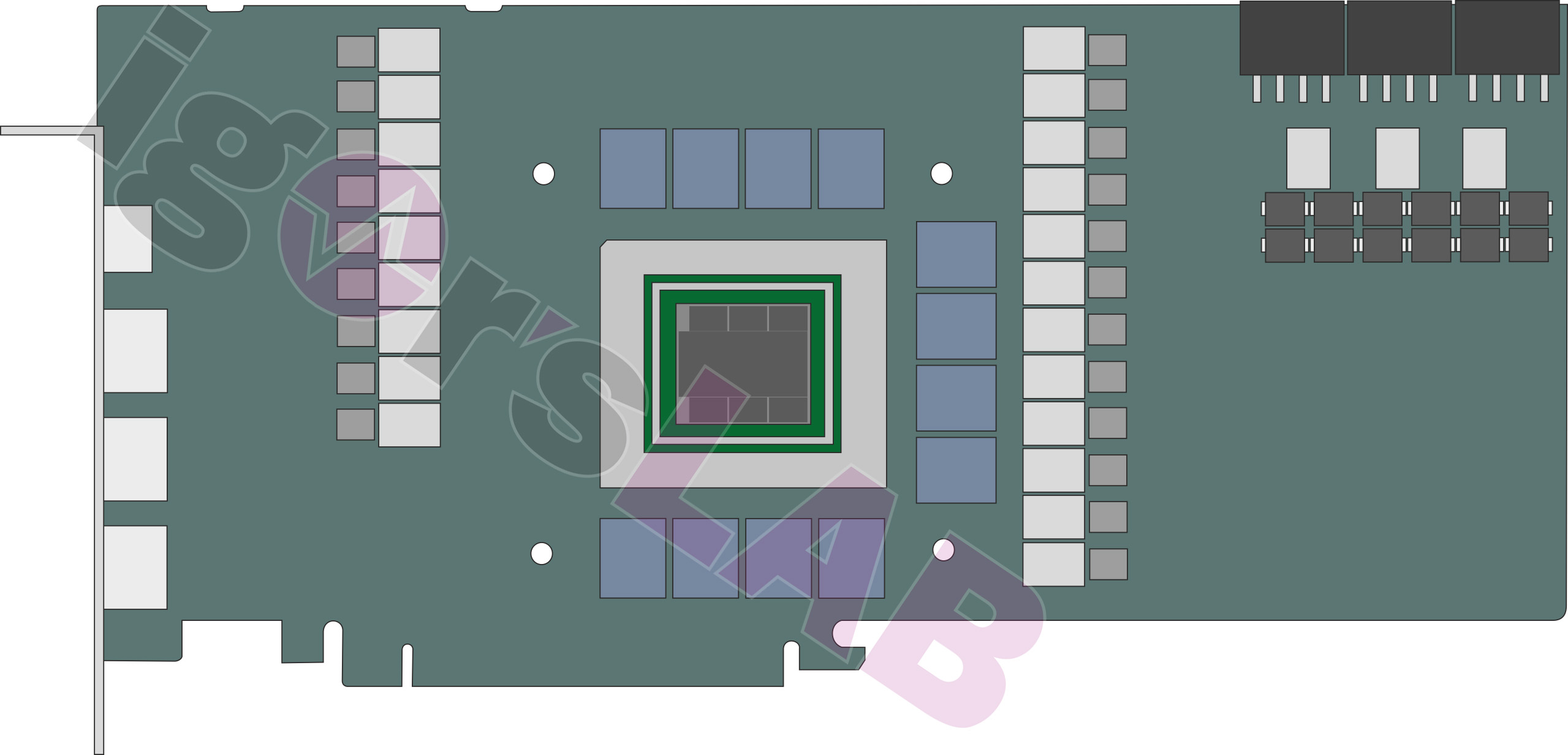
Let’s summarize what I noticed about all of the designs, which is based on CAD drawings, photos, and text descriptions:

  • The Navi31 GPU of the RX 7900XT relies on a total of 6 MCD chiplets and one GCD chip (I’ll leave the detailed data to the Twitter kings here, but they were quite good lately).
  • 12 GDDR6 modules are used, which suggests a memory expansion of up to 24 GB
  • There are (besides the usual low and partial voltages) 21 large voltage converters installed in my example, which could be divided as follows if AMD keeps the usual supply scheme: 16 voltage converters (from 8 phases running in parallel) for VDDC_GFX, 2x memory, 2x VDD_SOC and 1x VDDCI. The card would therefore be supplied with 8 phases, which is in line with the general trend (also at NVIDIA). By the way, this is not a speculation, but a real circuit design, but I do not want to go into detail.
  • In the left third there are the various voltage transformers for the partial voltages and below the voltage transformer row also the input filtering for the slot (12 volts and 3.3 volts), which I also left out for the reasons already mentioned.
  • We recognize 1x HDMI and 3x Displayport, USB-C is not on board
  • A total of three tracks on the external PCIe power supply supply the card’s voltage converters and each of the tracks has an LC combination of coil and upstream polymer caps as output filtering against high-frequency load peaks
  • In the presumed board design, we see three 6+2 sockets instead of the 12VHPWR. I’ll leave it open whether this PCIe 5.0 connector will make it onto the final cards.
  • However, this also limits the maximum board power of the card to 450 watts, whereby the actual TBP should be far below that.

As I wrote before, everything is in flow and can change almost daily. What I have included in the drawing is constant for a long time. It’s not quite complete yet, but it’s already somewhat meaningful.

Twitter contention?

Some time ago, I explained why the tweeted water level reports are often not worth the power that was used to feed the executing PC. The manufacturers are currently doing everything they can to camouflage, confuse and deceive. This has almost Putinian secret service qualities. And that’s exactly why I’m deliberately holding back with a lot of information at the moment. With some of them I know that they are true, but things can still change, with other pieces of the puzzle, skepticism prevails, whether something like this has not been purposefully scattered. The leaker business has become really tough. You are currently offered more than you would like to believe. The only thing is that you almost never know what you are actually posting. I stay out of such Twitter discussions, because it only falls on one’s feet unnecessarily anyway.


Kommentar

Lade neue Kommentare

Perdakles

Mitglied

43 Kommentare 20 Likes

Moin Igor, danke für die interessante Morgenlektüre. Mir ist aufgefallen, dass du im Text von sechs Chiplets sprichst, aber sieben abgebildet sind. Auch alle Gerüchte der jüngeren Vergangenheit sprechen von sieben Chiplets (1xGCD + 6xMCD).

Die TBP könnte durch den PCIE Steckplatz ja auch nochmal ca. 70W höher liegen oder?

Der Hinweis, dass die tatsächliche TBP selbst bei den Partnerdesigns nochmal weit unter dem theoretischen Maximum liegt ist eine sehr positive Neuigkeit. Das nimmt in der Branche ja sonst schon beängstigende Dimensionen an.

Antwort 2 Likes

Igor Wallossek

1

10,185 Kommentare 18,780 Likes

Ich sehe nur 6 Chiplets und einen Chip ;)

Antwort 3 Likes

big-maec

Urgestein

827 Kommentare 475 Likes

Liest sich schon mal gut von der Einschätzung. Ich hätte die RAM Chips um die GPU verteilt, jeweils 3 Stück an jeder Seite. Ist technisch Unfug.

Antwort Gefällt mir

Igor Wallossek

1

10,185 Kommentare 18,780 Likes

Die Tracks sind vorgeschrieben und links liegen noch jede Masse Ausgänge und Teilspannungen an. Das geht so nicht. Optik und Technik sind zwei paar Schule

BTW:
Ich habe den Chip/Chiplet Count noch einmal allgemeinverständlicher präzisiert :)

Naja, eher nicht ganz. Auch wenn MSI damit dann statt der 450 Watt immerhin 516 Watt bei der 3090 Ti schafft :D

Antwort 2 Likes

big-maec

Urgestein

827 Kommentare 475 Likes

Mein Gedanke hatte einen anderen Fokus. Mehr Platz zwischen den RAMs, eine andere Wärmeverteilung. Dagegen sprechen natürlich die technischen Aspekte und wie aufwändig das Ganze würde.

Antwort Gefällt mir

Igor Wallossek

1

10,185 Kommentare 18,780 Likes

Mehr Platz zwischen den RAMs bringt kühltechnisch nichts, verkompliziert aber den Kühleraufbau und das Mounting (Kräfte) :)

Antwort Gefällt mir

Unterfranke

Veteran

146 Kommentare 136 Likes

Chapeau!​

Manch Kommentar bedarf keiner langen Worte.

Antwort Gefällt mir

Göran

Veteran

154 Kommentare 63 Likes

Ein Vollausbau mit maximal 450 Watt TBP ... das kann man ja fast positiv bewerten.
Mich würde interessieren ob AMD die Strategie zu Messung der TBP ändert, um mit absoluten Gesamtwerten zu arbeiten und nicht Teilleistungen.
Ansonsten freue ich mich schon auf die Tests. Das wird ein interessanter Herbst für die Leser und viel viel Arbeit für Igor.

Antwort 2 Likes

Igor Wallossek

1

10,185 Kommentare 18,780 Likes

Nein, ich habe bisher keine Shunts "gefunden" und AMD wird sich sicher nicht in NVIDIAs Falle mit den Platinenverlusten begeben. Wer messen will, kann das ja auch extern machen. Die Auslesefraktion wird natürlich wieder heulen und diverse Faustformeln konstruieren. Ist halt so :)

Antwort 1 Like

RX480

Urgestein

1,871 Kommentare 862 Likes

Wieso nur 450W ?
... sollte net insgesamt 3x 150 +70 so ca. 520W sein (gabs ja so auch als 3090 OC zu kaufen)
(inoffiziell wird sicher mehr gehen)

Falls die AMDref. auf 450W geht und Customs offiziell auf 520W, sollte es doch reichen.
(mal schauen, obs dann auch 4-Slot -Designs werden wie bei der Konkurrenz, ... dann wohl mit dickeren 25mm Lüftern)

Antwort 1 Like

D
Deridex

Urgestein

2,213 Kommentare 846 Likes

Beim PCIe Grafikkartenslot sind es meines Wissens nach nicht 70W. Es waren, wenn ich mich recht erinnere, 12V und max. 5,5A was in meiner Rechnung 66W ergibt.

Aber auch 450W sind mir persönlich viel zu viel. Da bleibe ich lieber einige Stufen drunter und reduziere halt die Grafikeinstellungen.

Antwort 2 Likes

Igor Wallossek

1

10,185 Kommentare 18,780 Likes

Richtig, 66 Watt auf 12 Volt bei 5,5 A und knapp 10 Watt (3 A) auf der 3.3 V Leitung. Auch die wird für Kleinspannungen noch gern genommen.

Antwort 4 Likes

R
RX Vega_1975

Urgestein

575 Kommentare 75 Likes

Das Design soll ja von einer Custom Karte sein laut Igor
und denke dass selbst die AMD Referenz 7900 XT nicht über 375 Watt komplette Karte geht,-

Ob Anfang 2023 noch eine 7950XT kommt sei mal dahingestellt.

Antwort Gefällt mir

RawMangoJuli

Veteran

253 Kommentare 146 Likes

Sieht aus, als ob die unteren 4 VRAM Module wieder verklebt werden müssen xD

Antwort Gefällt mir

M
McFly_76

Veteran

396 Kommentare 136 Likes

Also ich glaube nicht dass AMD den 12VHPWR für die Stromversorgung der RX 7000-Serie verwendet.

Das würde auch bedeuten dass man sich ein neues Netzteil kaufen müsste um auf der sicheren Seite zu bleiben, da die PCI-SIG vor den PCI 5.0 auf PCIe Adaptern warnt https://wccftech.com/atx-3-0-12vhpw...r-safety-risk-using-adapter-confirms-pci-sig/

Antwort 1 Like

RawMangoJuli

Veteran

253 Kommentare 146 Likes

Angstronomics wird wohl richtig liegen.

Also kriegt zumindest die Ref. 2x 8PIN.

Antwort Gefällt mir

Igor Wallossek

1

10,185 Kommentare 18,780 Likes

Der Mist der PCI SIG zielt doch nur auf noch mehr Umsatz :D

Es geht auch per Adapter perfekt. Ich habs bis 600 Watt getestet. Läuft problemlos. Dass ich die 8-pin drauf habe, ist auch kein Zufall :D

Antwort Gefällt mir

Annatasta(tur)

Veteran

354 Kommentare 128 Likes

Kann man eigentlich auch zwei 600W Netzteile einbauen und dann zwei 6+2 an das eine NT und den Rest an das andere NT legen?

Antwort Gefällt mir

F
Furda

Urgestein

663 Kommentare 370 Likes

Wieso "Falle"? AMD und Nvidia haben zwei unterschiedliche Ansätze, aber beide sind nicht umfassend. Die Kombination von beiden wäre umfassend.

AMDs Art zu Rechnen ist für Tuning besser, weil man nur die Leistung der zentralen Komponenten misst und limitiert, ohne Beigemüse. Die total nötige Leistung ist jedoch ohne physische Messung unbekannt, und da kommen diese "Formeln" zum Zug.

Nvidia hingegen misst totale Leistung, suboptimal bei Tuning wegen Beigemüse und Verluste, dafür ist eine harte Totalzahl in Watt da. Zur PSU Dimensionierung die einzig brauchbare Angabe. Stichwort ATX 2.0 wiederverwenden bei ATX 3 Karten, hochaktuell.

Welche man bevorzugt, ist subjektiv, aber wieder tappt ja grün in die "Falle" und rot macht es angeblich besser. Nein, besser wäre die Kombination von beiden Varianten.

Antwort Gefällt mir

Danke für die Spende


Du fandest, der Beitrag war interessant und möchtest uns unterstützen? Klasse!

Hier erfährst Du, wie: Hier spenden.

Hier kannst Du per PayPal spenden.

About the author

Igor Wallossek

Editor-in-chief and name-giver of igor'sLAB as the content successor of Tom's Hardware Germany, whose license was returned in June 2019 in order to better meet the qualitative demands of web content and challenges of new media such as YouTube with its own channel.

Computer nerd since 1983, audio freak since 1979 and pretty much open to anything with a plug or battery for over 50 years.

Follow Igor:
YouTube Facebook Instagram Twitter

Werbung

Werbung