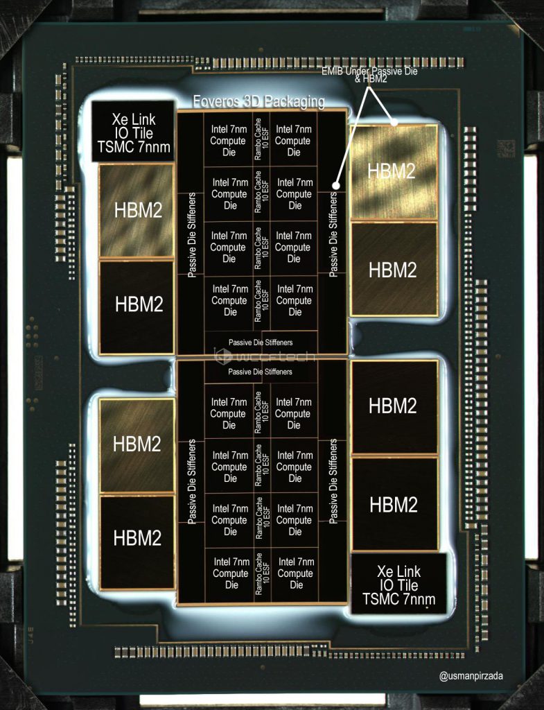
Intel recently unveiled one of its biggest chips, and our colleagues at wccftech.com have tapped various sources for more details. Although it was clear from the technical explanations at Intel’s Architecture Day what Intel is up to, the picture that now emerges is quite overwhelming. The colleagues show for the first time Intel’s 7nm die shot (of a packed product) including a complete and correct labeling of what to expect soon.

Intel’s Xe HPC 2-Tile (PVC) GPU uses a blend of Intel’s 7nm, Intel’s 10nm ESF, and TSMC’s 7nm process technology brought together in Foveros 3D packaging for this purpose. Everything the colleagues mentioned in their article has been confirmed by at least two of their sources, as well as cross-referenced, and represents the correct labeling for the Xe HPC Die Shot. The Intel Xe HPC 2-Tile package shown by Intel’s chief architect Raja Koduri (which is pretty much the equivalent of the Ponte Vecchio GPU in its early stages) is an absolute marvel in terms of the technology used.
The die-shot is nothing less than a technical demonstration of Intel’s most advanced process and packaging technologies. Not only does it show the first ever 7nm die (in a packaged product) from Intel’s in-house 7nm process, but it also shows EMIB in action along with Fovero’s 3D packaging. You can also see the promised mix-and-match philosophy with parts from TSMC and new features like Rambo Cache.

Let’s start from the top. The Xe Link/IO Tile can be seen in the top right and bottom right corners of the case and was manufactured using TSMC’s 7nm process. Interestingly, the die shot also contains two different sized HBM2 tiles that can be seen on either side of the main tiles. The focus of the two tiles is of course the compute die (16 in total), which is manufactured in Intel’s own 7nm process. The assumption that the vertical dies surrounding the compute die are either an XEMF Scalable Memory Fabric or Rambo Cache are so not true. The vertical dies on the right, left, top, and bottom positions are really just passive die stiffeners, but there is no logic to them.
The Rambo cache is actually in the middle and is manufactured on Intel’s 10nm Enhanced Super Fin process. The 10nm base die is actually under the tiles you can see in the picture. EMIB is located under the passive dies and the HBM2. Since this package is based on Intel’s 3D-Foveros technology, a lot of things are still hidden and as long as you don’t get a detailed 3D-diagram with the single layers, you can only guess the complexity of the package
Raja already revealed that there are 7 advanced technologies at play here, and colleagues interpret it that way:
- Intel 7nm
- TSMC 7nm
- Foveros 3D Packaging
- EMIB
- Improved Super Fin
- Rambo Cache
- HBM2
However, one must also keep in mind that the package shown is merely the first iteration (i.e., a prototype) of Intel’s upcoming Ponte Vecchio chip. Taking into account that this is due out sometime in late 2021 or early 2022, this sign of life shows that the company seems to be on a good path as far as its own roadmap is concerned. Ponte Vecchio will be used in the Aurora supercomputer, and there was a lot of concern beforehand about whether Intel would be able to meet the deadline at all. The answer to that, though, it seems, is yes.
Source: wccftech.com


17 Antworten
Kommentar
Lade neue Kommentare
Urgestein
Veteran
1
Mitglied
Mitglied
1
Veteran
Veteran
Mitglied
Veteran
Veteran
Mitglied
Urgestein
Veteran
Veteran
Urgestein
1
Alle Kommentare lesen unter igor´sLAB Community →