


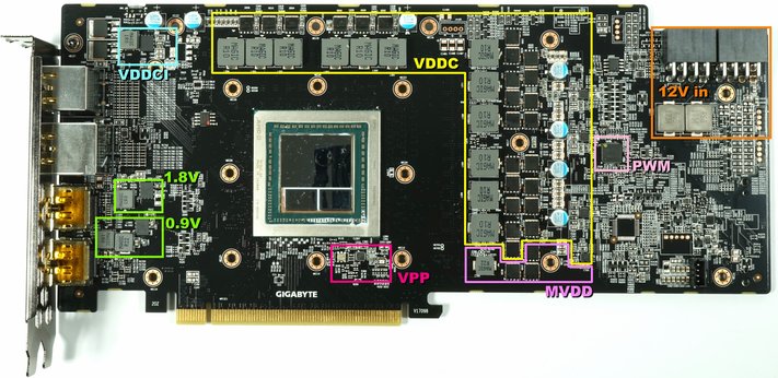
Board layout
Gigabyte is extremely different from AMD's reference layout of the RX Vega, which should also make the use of existing full-cover water coolers impossible. Also with the popular Raijintek Morpheus, end terrain is terrain, if you take a closer look at the voltage converter positioning for the GPU (VDDC).
Gigabyte also uses 6 phases with Doubling, resulting in a total of 12 voltage converters for the VDDC and one phase for memory (MVDD), but their positioning for third-party coolers poses real problems. The production of the further auxiliary voltages is also shown in the diagram.
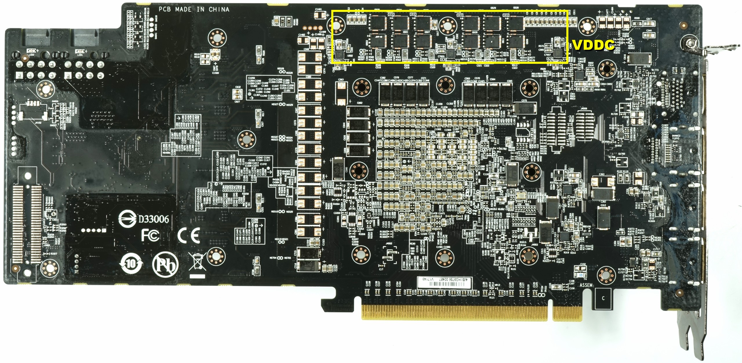
If you look at the back of the board, you can see that half of the most loaded low-side MOSFETS have gone right there. From this it can now be concluded that more than 30% of all voltage transformer losses occur, including the associated waste heat, on the back.
The whole thing can definitely no longer be removed cleanly from the front, but also requires a special cooling solution for the back. How Gigabyte solves this, we will see later and also test it.
Gigabyte relies on a total of two external 8-pin jacks. Since the motherboard slot is about 25 watts maximum, these two connections must therefore handle the rest. We'll see how much that is later.
In general, however, it has been noticed that gigabytes are many things that we still have on the development pattern or the reference board has simply been omitted. This starts with the Holtek microprocessor for RGB control (you can hurt) and ends with the dual BIOS (already more annoying). In the end, everything looks a bit like the savings version of a formerly quite ambitious project.
GPU Power Supply (VDDC)
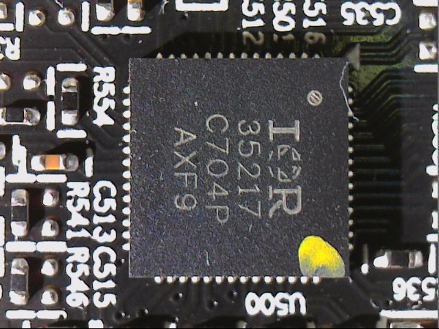
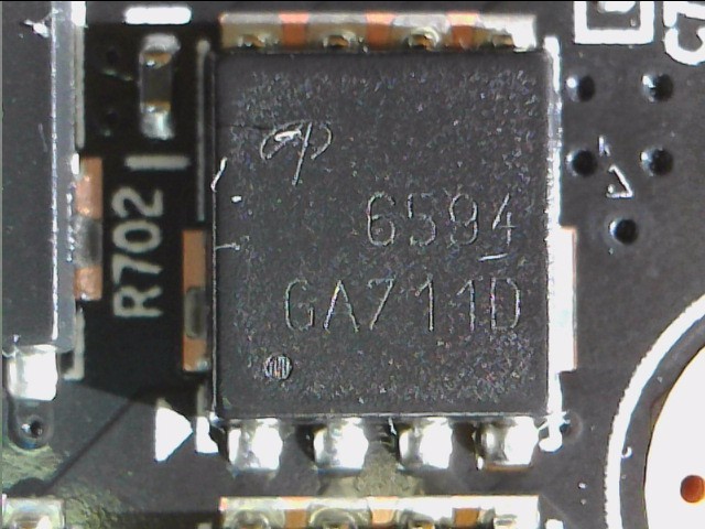
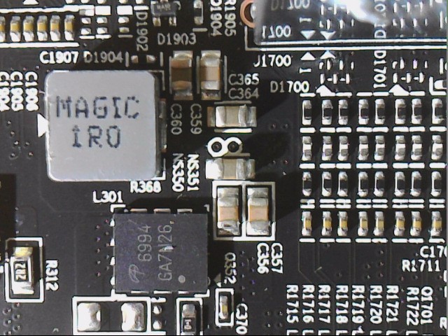
As with the reference design, the focus is on the IR35217 from International Rectifier, a dual output digital multi-phase controller that can provide both the six phases for the GPU and a wider phase for memory, which we are about to will come to speak. But back to the GPU and thus to what we see in the schema above as a VDDC block. We count 12 voltage transformer circuits, not six. However, since only six real phases are created, you double each of these phases in order to be able to divide the load into two converter circles per phase.
 |
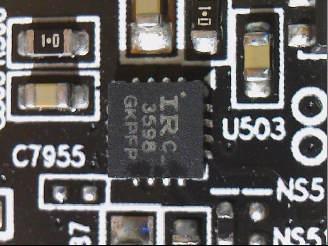 |
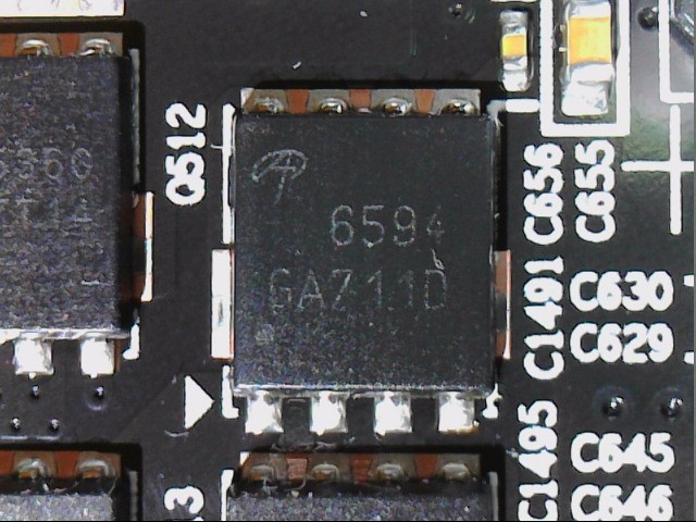
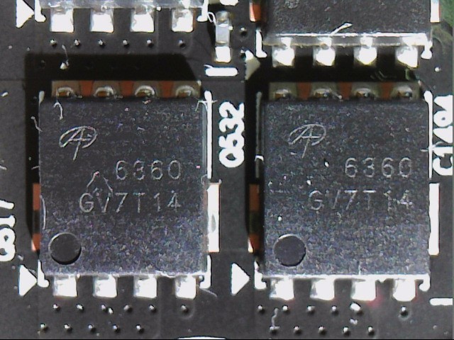
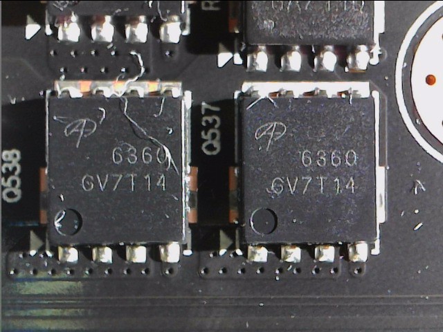
A total of six IR3598s are used for this so-called doubling, half of which are located on the front and back of the board. The actual voltage conversion of each of the 12 converter circuits is carried out by one AON6594 on the high and two parallel AON6360 on the low-side (all from Alpha & Omega). This is a favorable but acceptable component choice, especially since the parallel connection can also flatten the thermal hotspots.
 |
 |
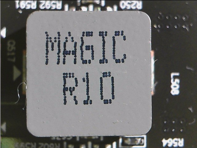
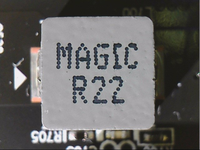
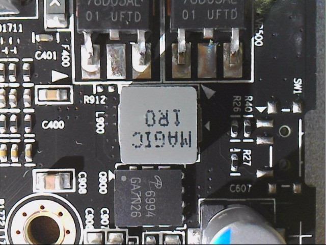
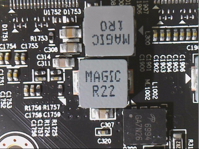
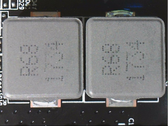
For the coils, Gigabyte relies on Magic Chokes from Foxconn for both the VDDC and MVDD range. With only 10nH for the VDCC, however, these encapsulated ferrite core coils are rather small. The coils for the one MVDD phase are on average at 22nH, even if 33nH has been sighted here often enough.
 |
 |
Power supply of the memory (MVDD)
As mentioned briefly, the IR35217 also provides one phase for storage. One phase is sufficient for the card, as the memory is much more sufficient. As with the VDDC, one relies on an AON6594 on the high side and two parallel AON6360 on the low-side (all from Alpha & Omega).
 |
 |
Other voltage converters
The creation of VDDCI (pictured bottom left) is not a big item in terms of performance, but it is important. It is used for GPU-internal level transition between the GPU and memory signals, something like the voltage between the memory and the GPU core on the I/O bus. In addition, a constant source for 0.9 volts is generated (picture at the bottom right). These two very similar voltage converters each rely on an asymmetric dual-N-channel MOSFET AON6994 from Alpha & Omega.
 |
 |
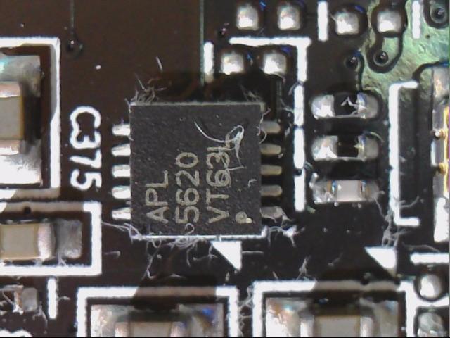
In addition, there is also a 1.8V source (TTL, GPU GPIO, image at the bottom left) on the front side, which is identically equipped with an AON6994. Below the GPU you can still find the APL5620 from Anpec for the VPP. This ultra-low dropout chip generates the very low voltage for the PLL area (Phase Locked Loop, image at the bottom right).
 |
 |
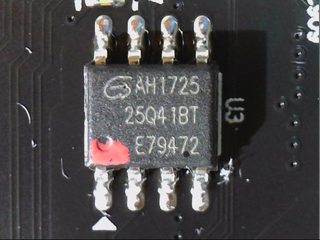
So we would almost be through, because the rest is the usual standard. Only the stand-alone BIOS chips 25Q4, which is a simple SPI flash chip, are still striking. Gigabyte has simply saved the switch, as well as the second BIOS chip, even though it is provided on the board (and thus possible).
In the entrance area there is a ferrite core coil with 68 nH for the input filtering, which helps to block the occurring load peaks including the incidental products of power supply.
 |
 |


Kommentieren