


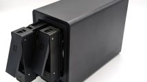
Since I wanted to disassemble the card for the board analysis later anyway, I just anticipate the usual procedure. AMD really didn’t save on screws for the single-slot design, so you turn and turn and turn…. Done! Let’s take a closer look at what AMD has packed into the Radeon Pro W7600.
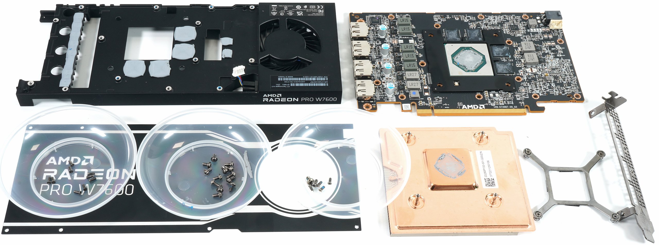
Teardown: Board and components
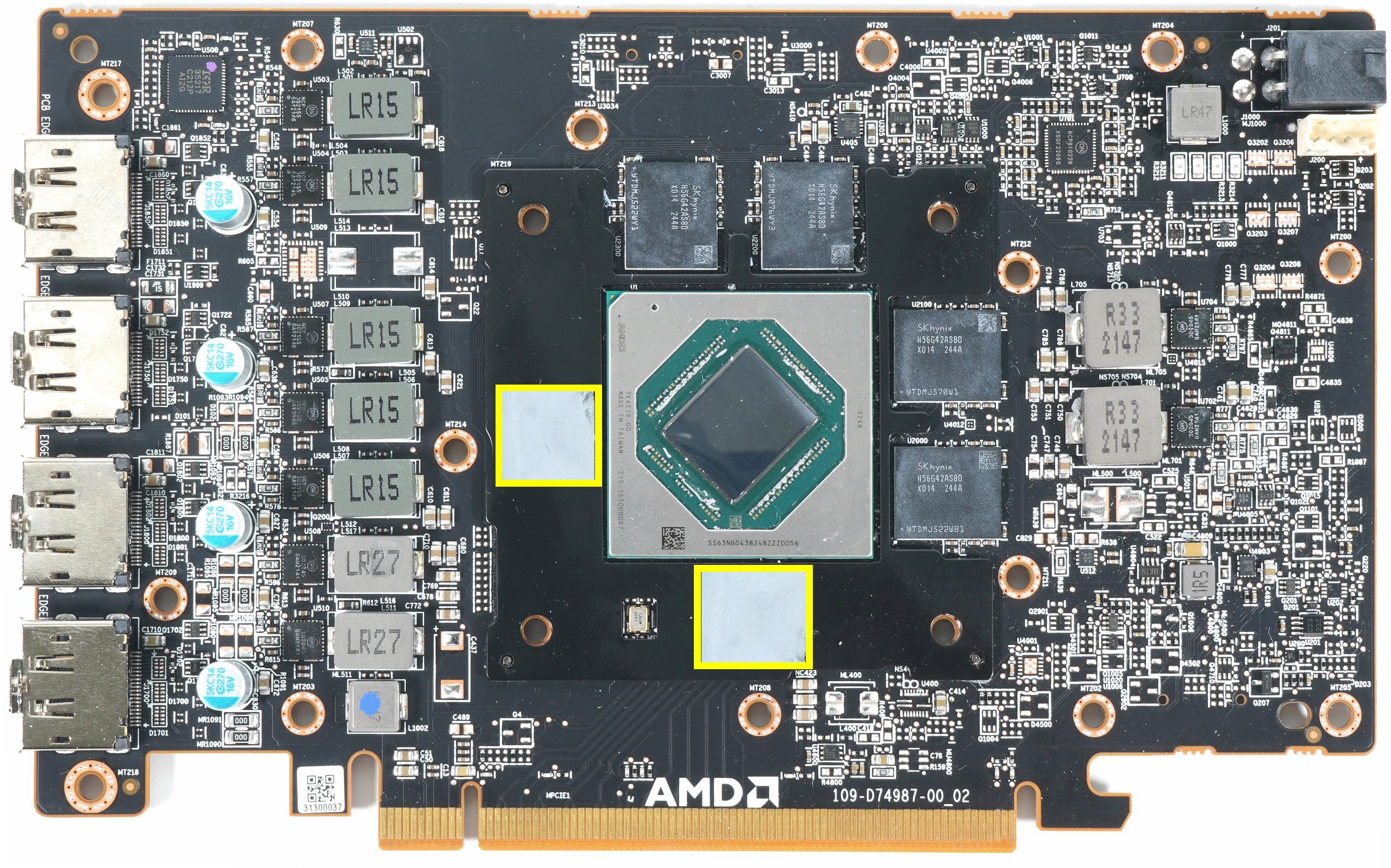
let’s start with the power supply. AMD puts the whole thing on a 2-way socket, from which an internal cable leads to the 6-pin connector. That’s not particularly nice, but it can be done that way. The two cables (12V and ground) can easily handle the approximately 70 watts. Behind the socket as well as at the PEG there are directly larger filter coils against the spikes, but you can’t find larger capacitors or fuses. The board relies on a total of 5 phases for VDDCR_GFX (one less than the Radeon RX 7600 MBA), which is the GPU voltage. The used IR35217 from International Rectifier (we also know this part from many motherboards) is a dual-loop digital multi-phase buck controller and in the layout used here AMD does without doubler chips and works with a total of five real phases for VDDCR_GFX and two phases for VDD_SOC.
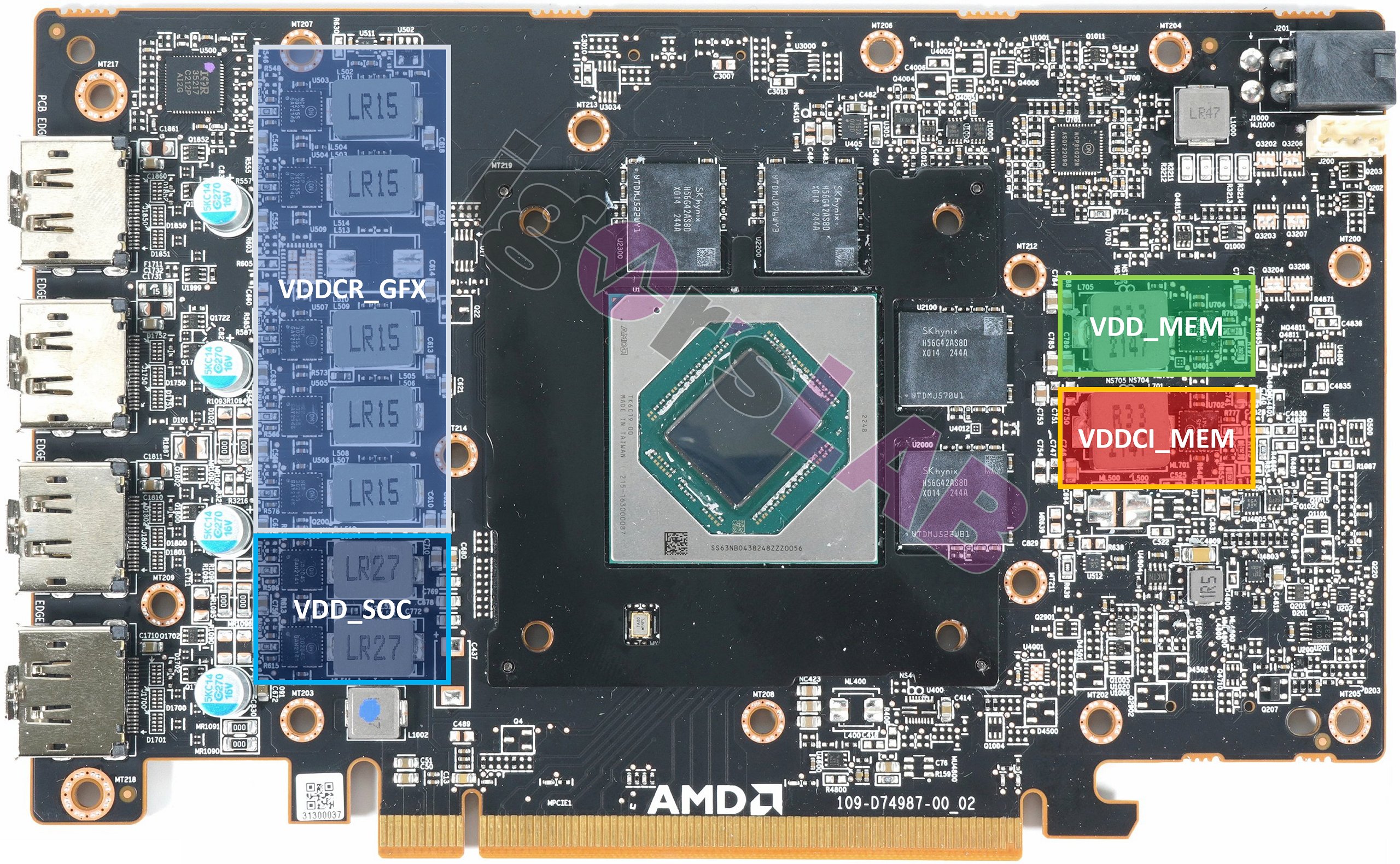
In addition, there are two phases for SoC and one each for the memory (VDD_Mem) and VDDCI. The generation of VDDCI is not a big item in terms of performance, but it is important. It is used for the GPU-internal level transition between the GPU and the memory signal, something like the voltage between the memory and the GPU core on the I/O bus. An NCP81022 works here as a second PWM controller, also for VDD_MEM. In addition, one generates other constant sources for various partial voltages. An ultra-low dropout chip generates the very low voltage for the PLL (Phase Locked Loop) area.The rest of the extra-low voltages I leave aside here for lack of relevance.
The used DrMOS for VDDCR_GFX are rather cheap products from OnSemi. The NPC302155 with 50A peak current integrates a MOSFET driver, a high-side MOSFET and low-side MOSFET in a single package. The other voltage converters rely on the slightly weaker NCP3020445 with 45A peak current in the same design. This chip is specifically designed for high current applications such as DC-DC buck power conversion applications. This integrated solution reduces board space requirements compared to a discrete component solution. The coils used for VDDCR_GFX have an inductance of 150 nH, the others of 270 nH (SoC) and 330 nH (memory).
The cooler
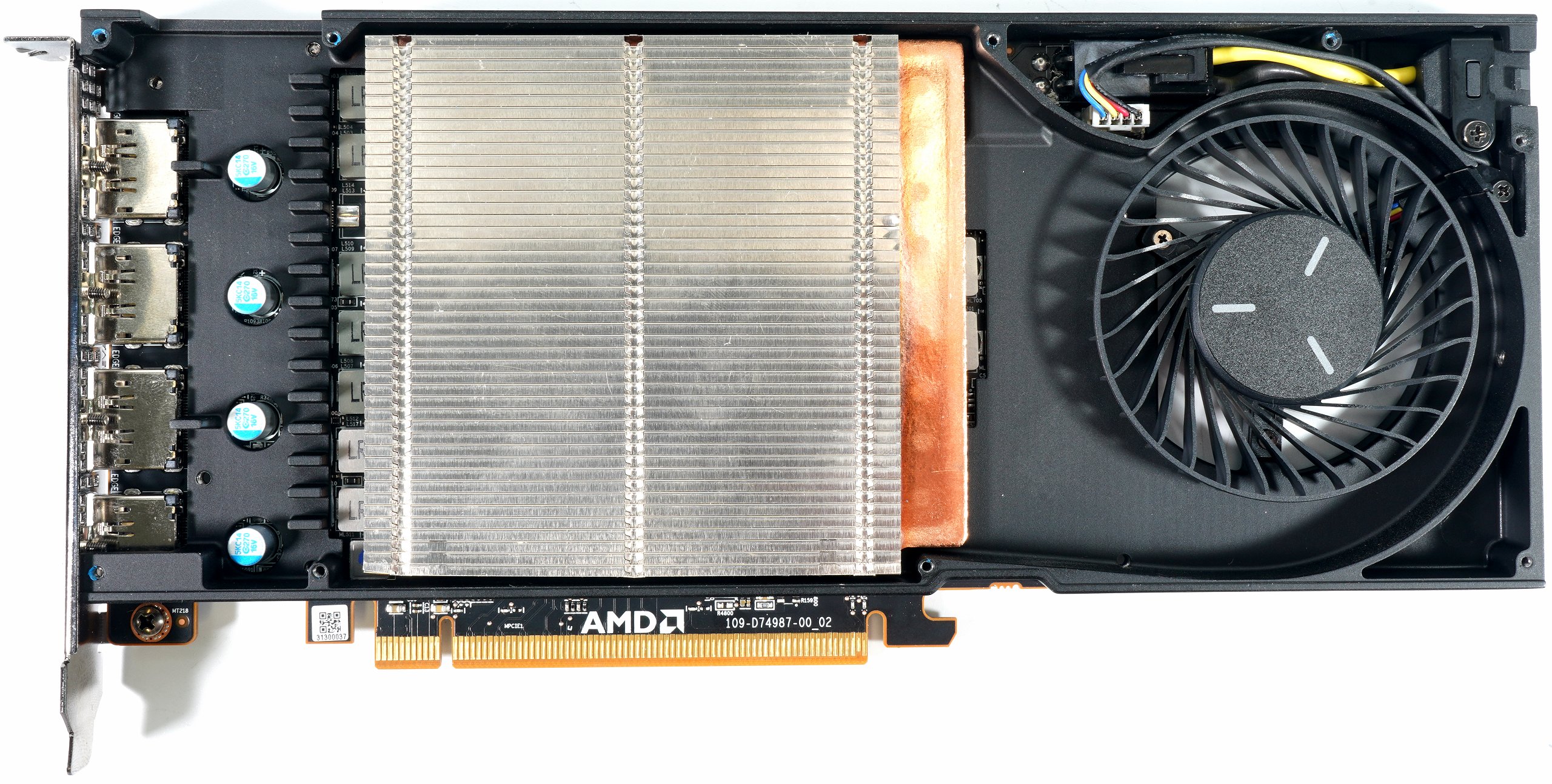
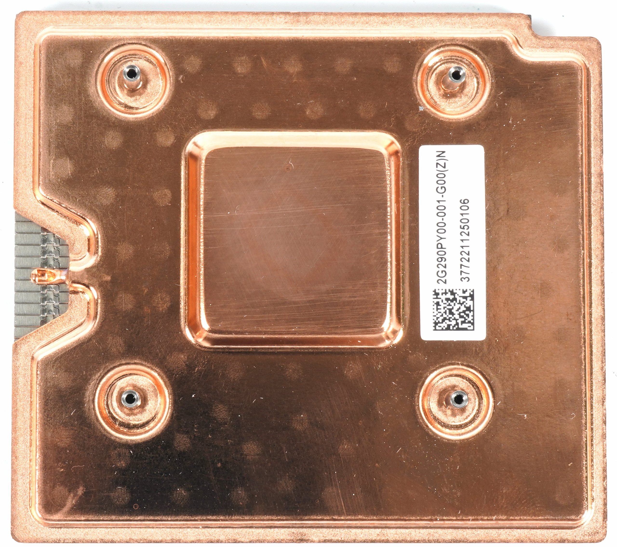
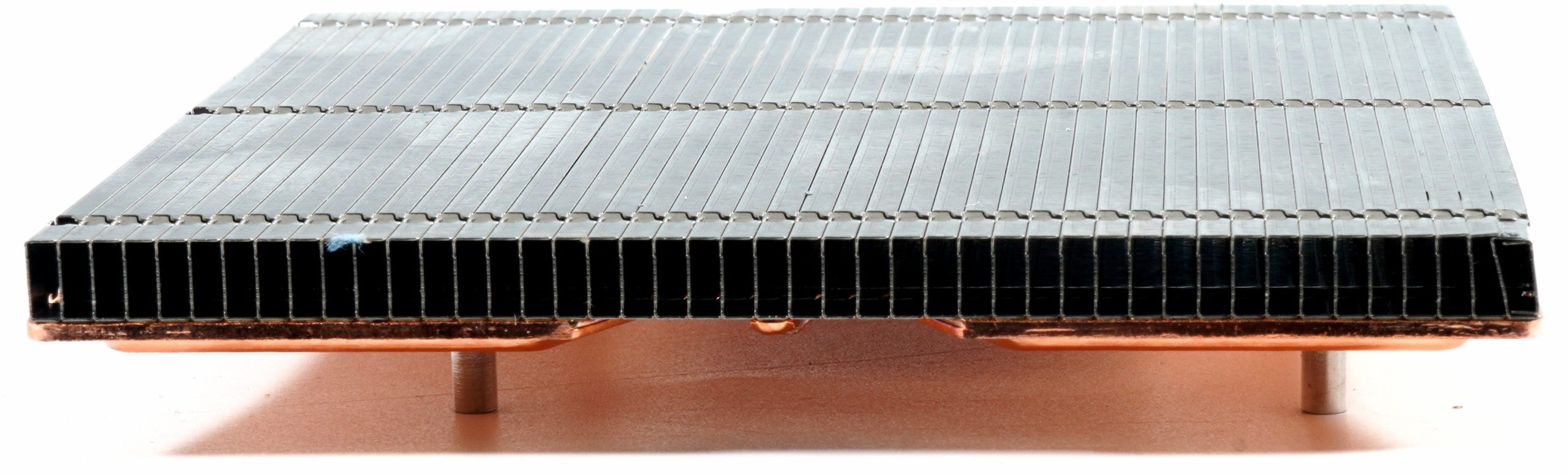
Opening the lid at the front, we can see the flat cooler design with the vapor chamber as the central element as well as the radial fan for the cooling air. Beyond that, we also see the great cable to the 6-pin socket at the end of the card. There’s not much else to discover, so let’s turn the fun around and take out the Vapor Chamber, which is only screwed to the board, so it sort of “floats” like NVIDIA. This is perfect for leveling out the tolerances of the GPU and memory, as the latter only rests on the frame, but not on the chamber.
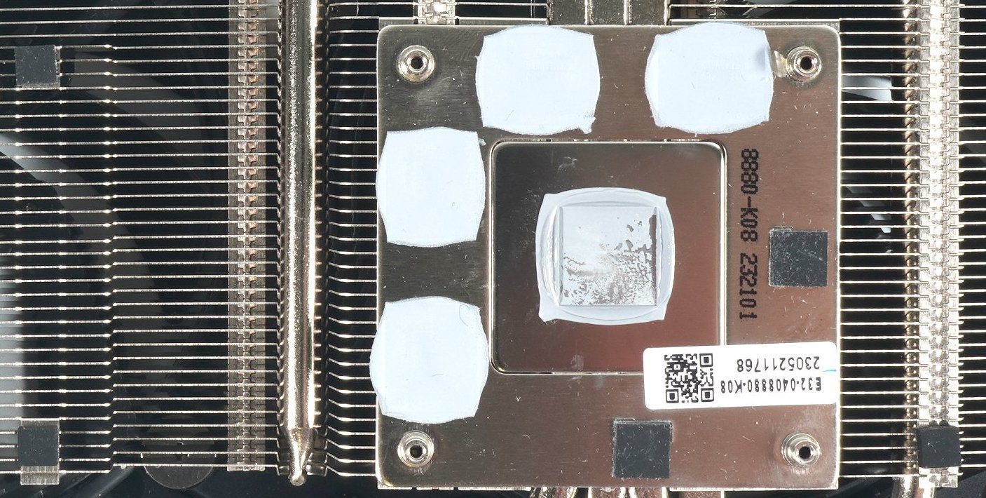
This is exactly what we see on the back. On top of that, there are four board-hard pads for the VRAM, which I don’t particularly trust, but more on that later. Also, all the voltage converters are thermally attached to this frame with thicker pads.
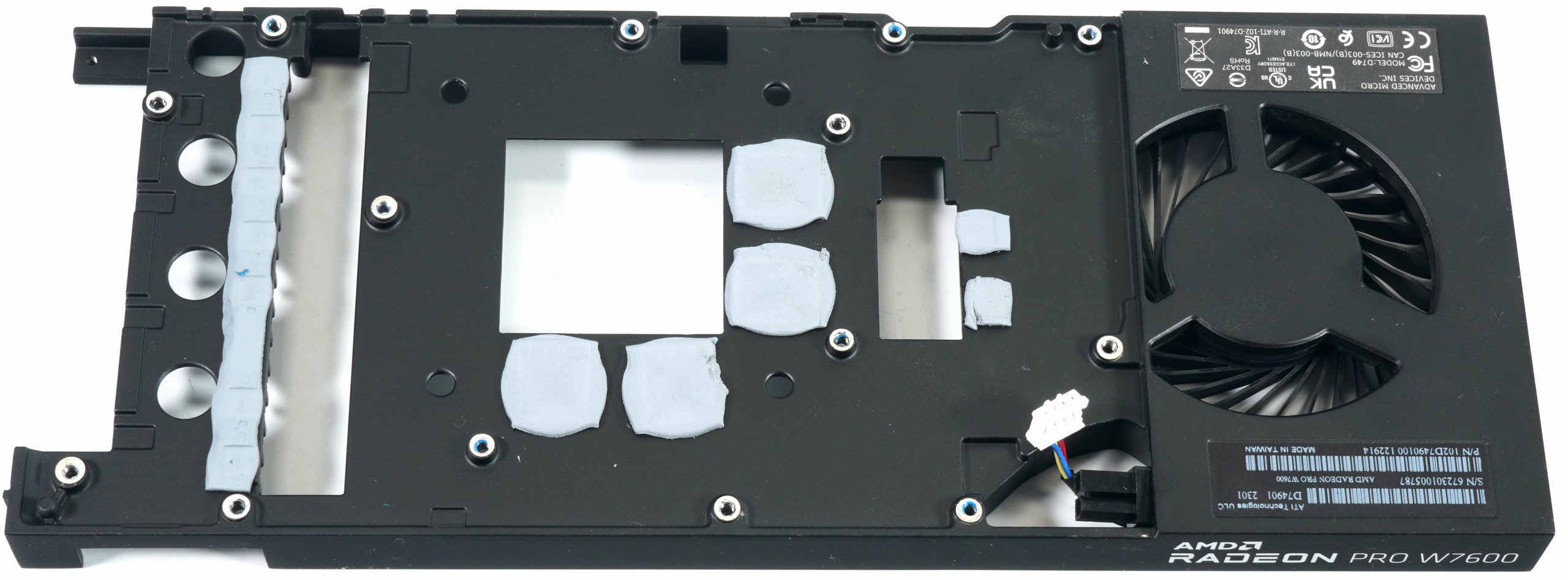
However, there is a problem with such thick pads if they are used on one side as they are here. If you screw the board tightly to the frame, it will inevitably warp and the vapor chamber will start to tilt because it is no longer flat. The result is a very different contact pressure on the GPU. AMD must know this, because otherwise they wouldn’t have screwed a stabilizing plate around the GPU socket. However, that is not enough because the holes for screwing the board sit much further out. You could have helped yourself with a properly sized additional thin pad (or two) on the empty areas of stabilization (see picture below), but you didn’t. I did.
The board partners prove that this is not a miracle with the equivalent RAM configuration. Simple spacers are used and the world is all right again! Here is an example from MSI, where they even use five (!) spacers for correction and securing, two of them alone for the memory directly at the heatsink. That is common sense and falls into the basics category.
The vapor chamber isn’t particularly large, but offers enough surface area for the fin heat sink on top.
The air is pressed through this and transported in the direction of the slot bracket. All this is not witchcraft, anything but new and has been practiced in this form for years. And yet, you now have to ask yourself why the card already fails at 125 to 130 watts.
I didn’t find any faults for the time being and therefore decided to cool it a bit differently or to exchange pads and thermal paste.


91 Antworten
Kommentar
Lade neue Kommentare
Veteran
Mitglied
Mitglied
Urgestein
Urgestein
Urgestein
1
Urgestein
1
1
Urgestein
Veteran
1
Veteran
1
Urgestein
Urgestein
Urgestein
Urgestein
Alle Kommentare lesen unter igor´sLAB Community →