I had opened a can of oil sardines from MSI the other day, but I already wrote it in the previous article that these consequences of thoughtless profit maximization affect almost all manufacturers. The topic was also the composition of heat conducting pads and the consequences of bleeding too much silicone. Nevertheless, I sat down to write another kind of follow-up, because the circle of bent circuit boards and misunderstood frugality closes seamlessly here. And that’s exactly what you have to talk or write about.
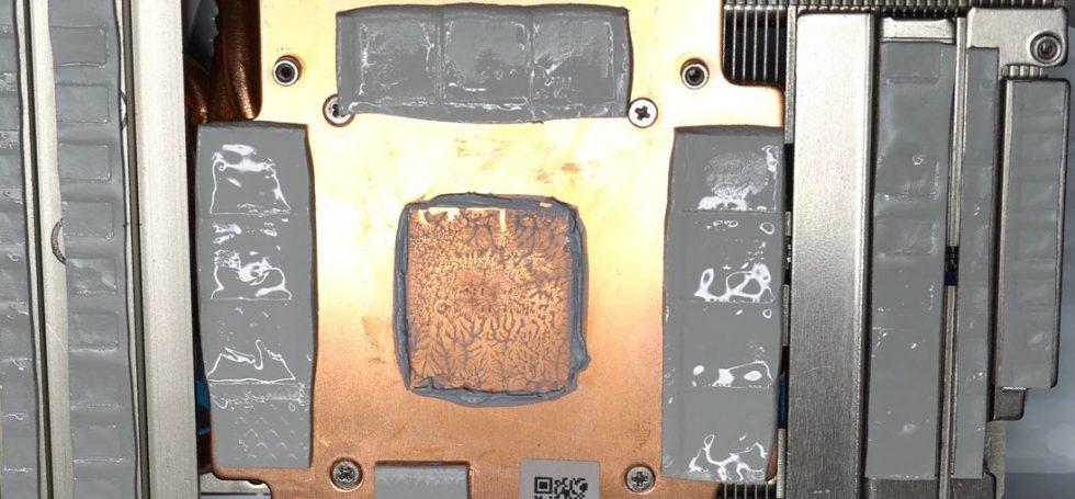
Gap dimensions for the Ampere cards – Die, Package and PCB
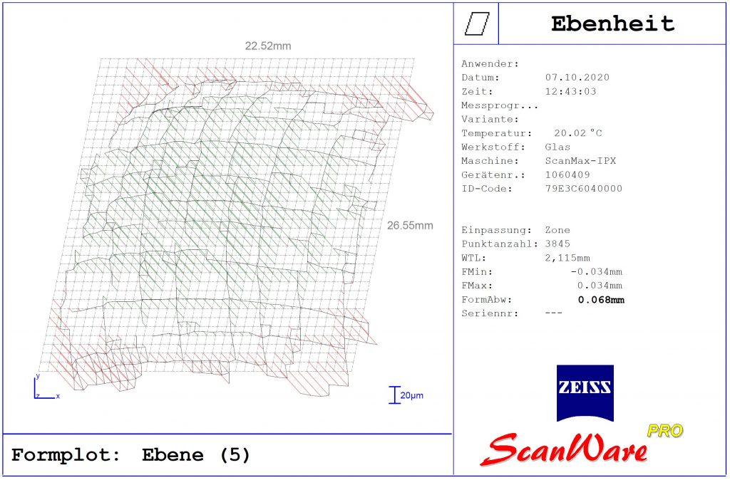
The big Ampere chips are bent, I already reported about that in detail. Here the cause was and is to be sought in packaging, but I will come back to that in a moment. The concave curvature was already present on Turing, but not as extreme, and the overall height of the package was also much more uniform. In order to prove this, we once measured a rather average graphics card at 20 °C room temperature. The curvature of the die is here with 0.068 mm (according to NVIDIA within the specifications) still in the tolerable range, but I also had a card with something over 0.08 mm. This can still be managed quite well with thermal paste, if it doesn’t turn out too liquid, and in the end it also differs only slightly from Turing. Here is the shape plot for flatness:
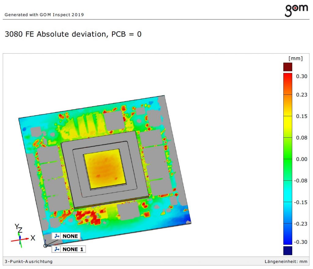
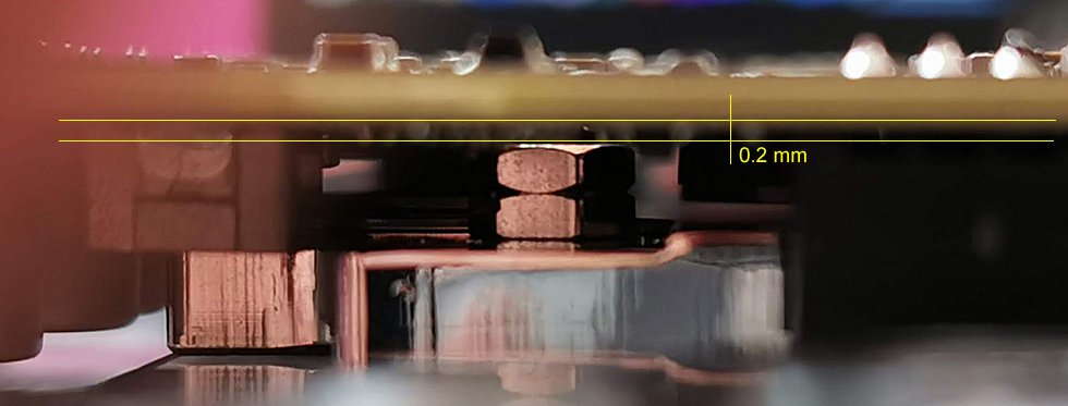
At the same time, I also scanned a (supposed) extreme case myself in 3D high-resolution. Here, however, the curvature in the die is 0.08 mm and more in places, which certainly raises questions as to how such a thing can occur. Often enough, the whole board (including package!) is already warped like on my scan of a GeForce RTX 3080 (the black represents the cooler bottom and the plane). In such a case it is also very difficult to achieve an exact centering and instead of the 0.08 mm of the die as such there is suddenly a gap of 0.156 mm on one side
A package also always has stresses and certain height tolerances, so this is still completely normal. However, NVIDIA specifies a tolerance range of up to 0.3 mm, which is also very high compared to Turing. We remember: there were waterblocks of German premium manufacturers, which only used thermal paste between the RAM modules and the cooler bottom instead of thermal pads (< 0.15 mm). The excellent results are well known and have also been proven by my tests. I’m afraid that’s no longer possible.
The following evaluation of the height differences shows a bulge and a simultaneous deviation of the actually measured heights from the 3D construction file, which I have placed underneath as a direct comparison. You can also see very well the bending of the package and the underlying board of the graphics card. In this case, we see that even the circuit board had to bend significantly due to the screwing in order to be able to make contact at all. By the way, this is already irreversible after cooling down after a BurnIn.
So I see a deviation of about 0.3 mm from the norm, which NVIDIA considers to be a tolerance limit, but still practicable. This 0.3 mm doesn’t sound like much at first, but in practice you now get a problem. Now, of course, you could force the board down by screwing it tight, but that’s not really smart. Everything will warp all the more and the surfaces will also no longer be able to lie flat on each other (memory, MOSFETS, etc.).
Here you definitely have to switch to the next thicker thermal pad and it also explains why the pads are so thick this time. So the 1 mm thick pad suddenly becomes a 1.5 mm or 2 mm thick pad with higher thermal resistance and the known consequences for cooling. But what should the cooler manufacturer do, because the next package can already look completely different? So you go for pads that are thicker than needed on average, while being extremely soft to minimize pressure on the memory in the case of a less curved board. But that is precisely where the problem lies. Please keep scrolling.












124 Antworten
Kommentar
Lade neue Kommentare
Urgestein
1
Mitglied
Mitglied
Urgestein
Urgestein
Urgestein
Veteran
1
Mitglied
Veteran
Urgestein
Urgestein
Mitglied
Veteran
Mitglied
Urgestein
Urgestein
Mitglied
Alle Kommentare lesen unter igor´sLAB Community →