Today I have a glimpse into the near future of RAM technology for you, and as is so often the case in the computer hardware industry, it comes from China, where SK Hynix’s new DDR5 memory ICs are already available for purchase today. With a proxy like Superbuy, some patience and even more trust, you can import such a Hynix A-Die kit to Germany and taste what the masses of enthusiasts can expect at the end of the year.
Unboxing and PCB analysis
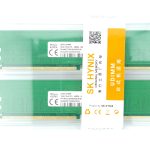
The modules are quite unspectacular DDR5 sticks with a green PCB and in JEDEC format, which are simply packed in a carrier frame made of transparent plastic. You only see that this is something special and new when you look at the sticker with the specifications. DDR5-5600 is shown here, mind you as a JEDEC profile without XMP. For context, previous DDR5 kits always included a JEDEC profile of DDR5-4800, so 800 Mbps less.
If we remember the DDR5 deep-dive interview with Kingston just under a year ago, where jumps of 400 Mbps per year were expected, then the new memory components from Hynix already double this expectation – but that is only on the sidelines.
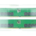
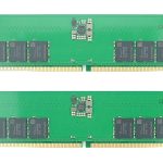
Apart from the spec sticker, the modules could hardly be more inconspicuous: Single-ranked with 8 ICs and a PMIC populated on one side, according to the DDR5 A0 JEDEC reference layout. Only a black imprint with the letters CX22Q3 on the upper right is really noticeable. RGB or other gimmicks are out of place here.
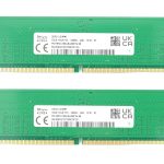
On the sticker we can find manufacturer SK hynix KOREA, module type DDR5 UDIMM, specifications about capacity 16 GB, rank count 1, bit organization x8, binning 5600B, board UA0 and temperature rating XT, as well as part number HMCG78AGBUA081N BA and serial number of each module. Furthermore, CE and UKCA conformity marks, a barcode and QR code can be found here, which should contain all this information encoded once again.
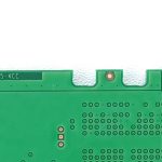
Unfortunately, we don’t find a layer indicator on the edge of the PCB, but we do find some other noteworthy markings. First, as usual, there is the 94V-0 designation and the Underwriter Labs logo as safety certifications for the North American market. What the markings L3 and the G mean here, I can’t say exactly. Behind the A0c could be the PCB layout, based on A0 from JEDEC. At the other end of the IC side, there is only a very small gold embossing with the identifier S1462401 and no other information.
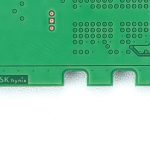
On the back of the board there is an imprint of the manufacturer SK hynix on the edge and another coded identifier 2215-4CC, whereby the former probably stands for the manufacturing week of the pcb.
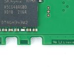
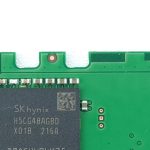
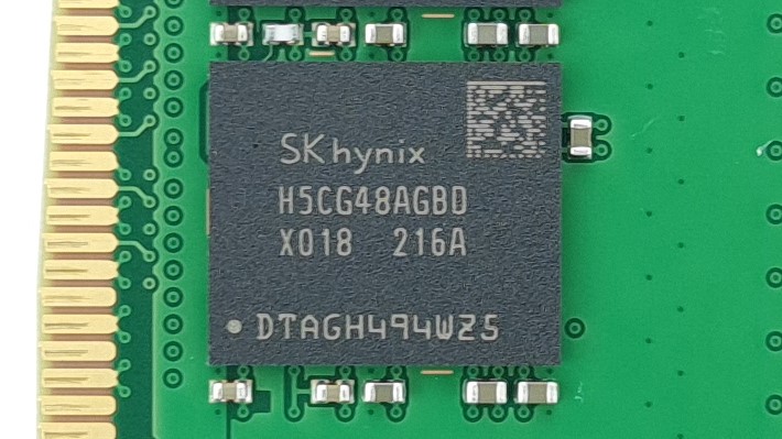
The ICs have the identifier H5CG48AGBD X018 216A, where the A in the first part is decisive for the recognition of the new stepping. Unfortunately, SK Hynix still hasn’t put an updated DDR5 IC part number legend online yet, but I’ll try my hand at an interpretation based on the DDR4 legend:
- H5C: SK hynix DDR5
- G4: Storage density – 16 Gbit
- 8: Bit organization – x8
- A: Generation/Stepping – 2. resp. A
- GB: Binning: 5600 46-45-45
- D: Operating temperature – 0-95 °C
- X: reserved
- 018: Package option: 78 ball, single die
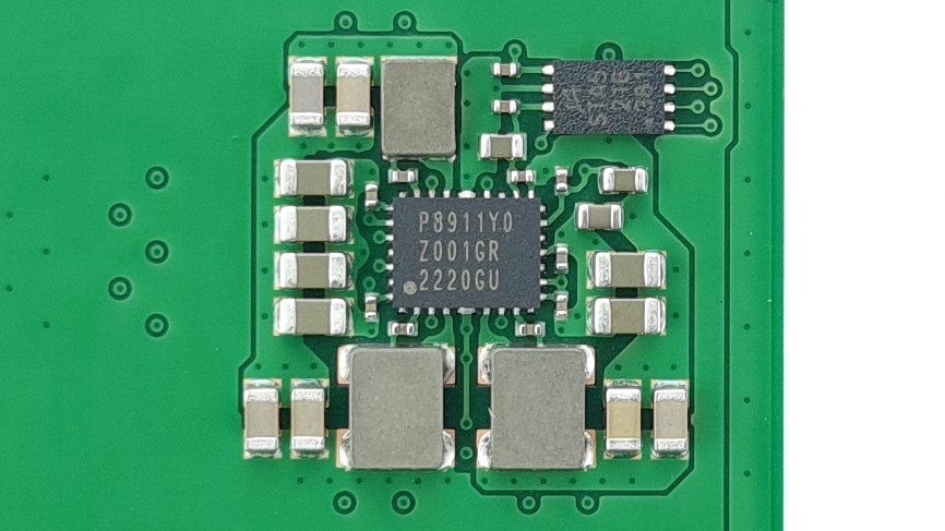
The PMIC is an old familiar one, the P8911Y from Renesas. This “JEDEC PMIC” is installed on various JEDEC DDR5 modules and is characterized by the fact that it can now be unlocked on most boards and thus be coaxed to more than the normally limited 1.435 V VDD and VDDQ. Of course, the modules don’t have a heatsink, so if you want to go far beyond the 1.1 V standard voltage, you also have to take care of the cooling of the modules.
The ICs are almost identical to SK Hynix’s predecessors, M-Die, both in dimensions and part number. The only real difference is the A instead of M in the code. This counting method is common in the production of semiconductors and especially flash memory, where the letter M is introduced to the normal alphabet. Accordingly, Hynix’s next IC would be a B-Die. If anyone can explain to me where this counting method comes from, feel free to let me know in the forum! 😉
As mentioned before, there is no layer indicator on the board, so I have to use the good old sandpaper again. After a short time, an 8-layer design is then used on the upper edge, which should effectively become the new standard for DDR5 kits from 5600 Mbps.






41 Antworten
Kommentar
Lade neue Kommentare
Veteran
1
Urgestein
Urgestein
Urgestein
Mitglied
Veteran
Veteran
Mitglied
Urgestein
Veteran
Urgestein
Urgestein
Urgestein
Veteran
Mitglied
Veteran
Urgestein
Alle Kommentare lesen unter igor´sLAB Community →