


Board, power supply and components
The KFA2 board has a 12-layer board with backdrill process that I already described in spring 2020. The type of power supply for the GA102-225 is again analogous to the other cards with the GA102. If we take a look at the top side of the board, we immediately recognize the division of the main power supply into two parts. NVDD (blue) stands for the conventional core voltage, i.e. what we like to call GPU voltage. And yet, this board is slightly different from the GeForce RTX 3090 reference board.
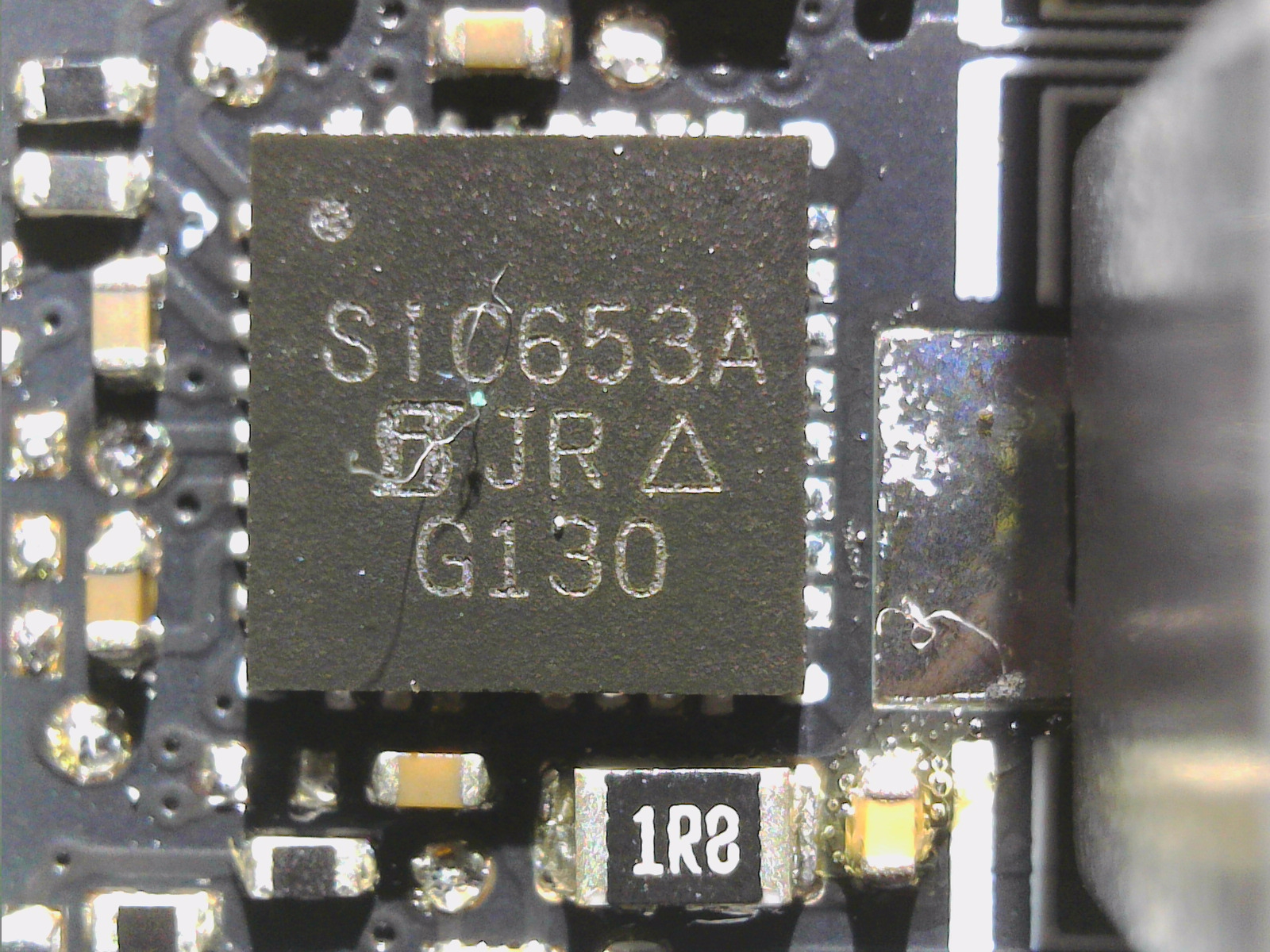
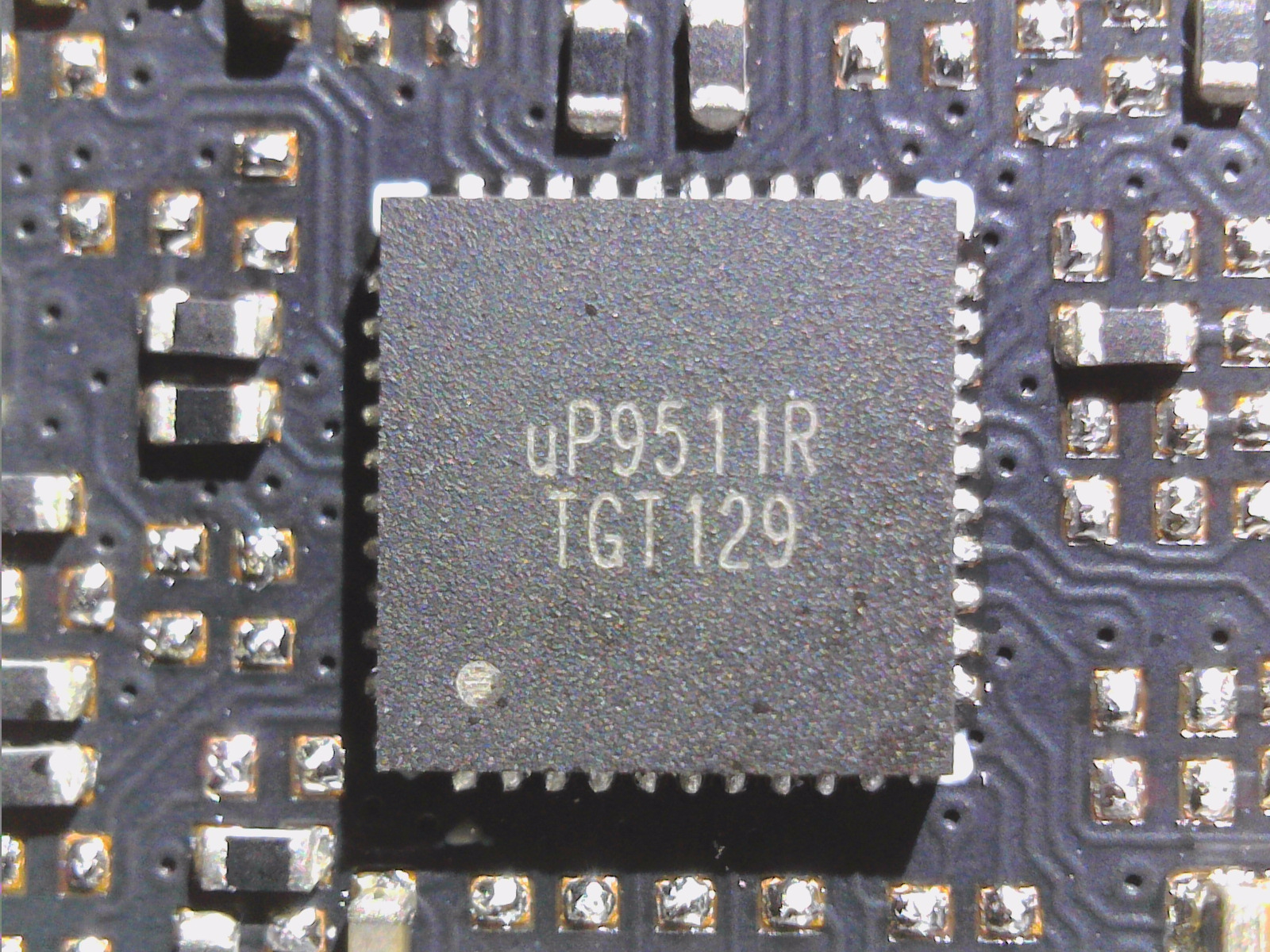
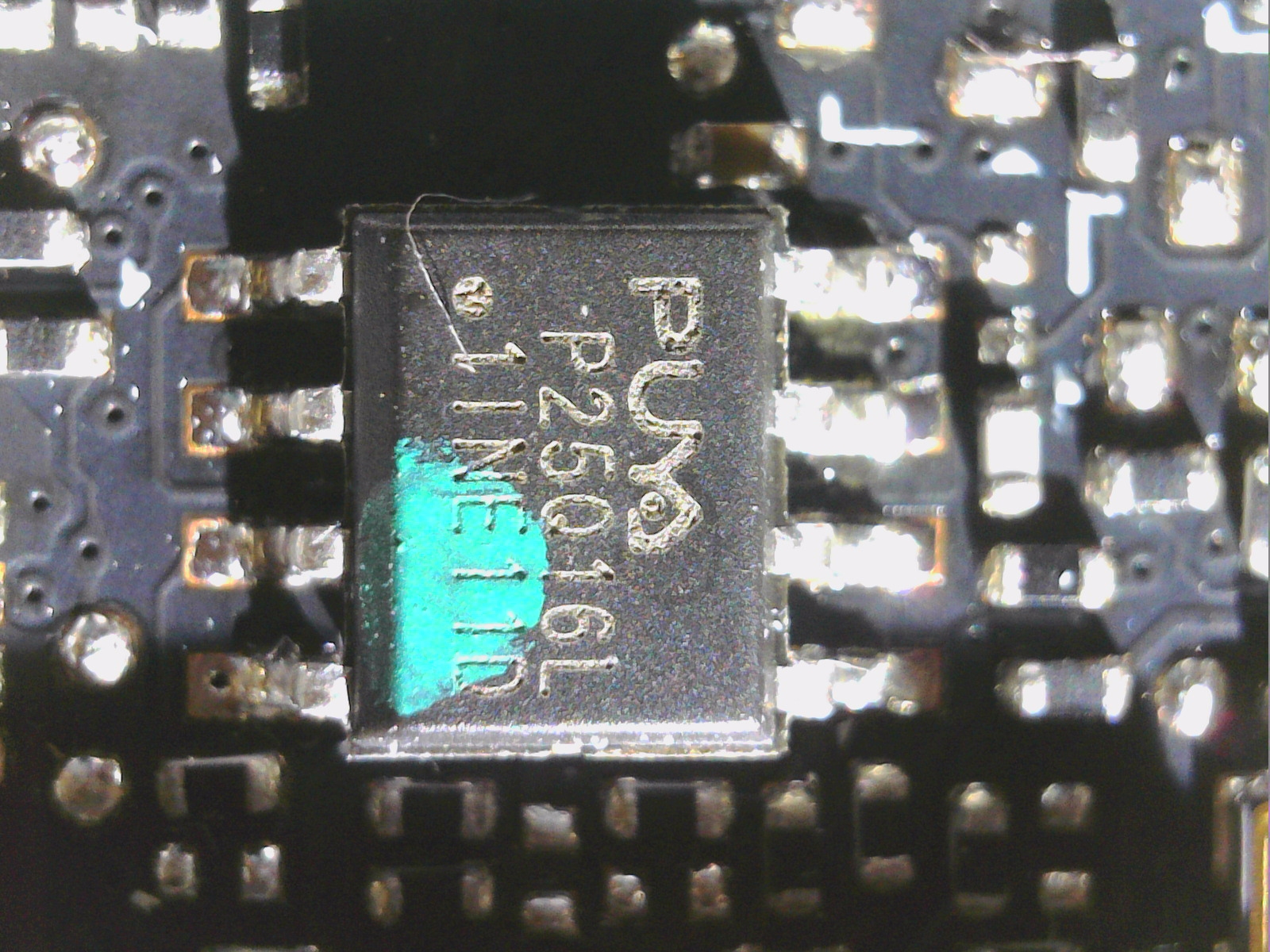
Here, there are now a total of 10 instead of nine individual phases for NVDD, which are provided by a uP9511R on the rear (blue). This is a digital PWM controller with VID interface, compatible with NVIDIA’s Open VReg specification. The 10 phases are each implemented with Vishay SIC653A Smart Power Stages (SPS), which also enable MOSFET DCR. The SIC653A is an intelligent device that combines a
high-side and low-side MOSFET and a high-power driver with an integrated bootstrap FET. The SIC653A provides high accuracy high precision current and temperature monitoring (IMON and TMON) that can be fed back to the controller and doubler to implement a multi-phase DC/DC system.
The assembly of the power supply MSVDD (green), which I had called “Gedönsspannung” and which stands for “Miscellaneous”, has a similar structure. We still find a total of five (instead of six in the RTX 3080) individually controlled phases generated by a uP9511R UPI (rear). The five PLCs again rely on the SIC653A from Vishay. In the end, there are 14 phases for the GPU alone and the various voltages to the same. This should also make power gating in the GPU a bit easier, whereas AMD uses a similar, albeit much smaller, swap with VDDCI. The voltage range of both ranges is between 0.7 and a maximum of 1.2 volts, whereby the maximum value can never be reached by the end user without special firmware and software.
The shift of the added control circuit for NVDD to the left also makes sense thermally, because one more phase not only takes into account the TBP in the power limit, which has increased by up to 30 watts, but it also reduces the power dissipation of each individual phase, because the switching frequency also seems to have been adjusted. If you calculate about 5 to 6 watts for the two additional memory modules, then NVDD will certainly account for about 20 watts more, the rest of 4 to 5 watts is for MSVDD.
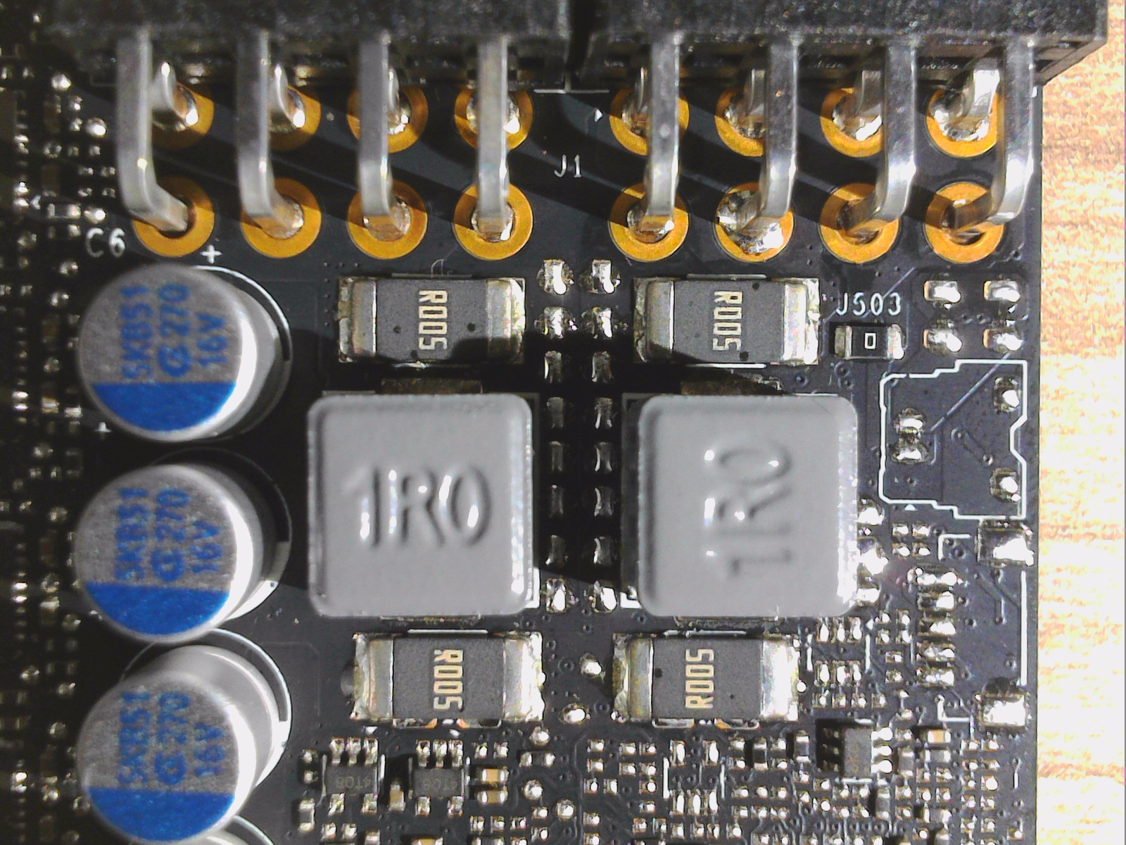
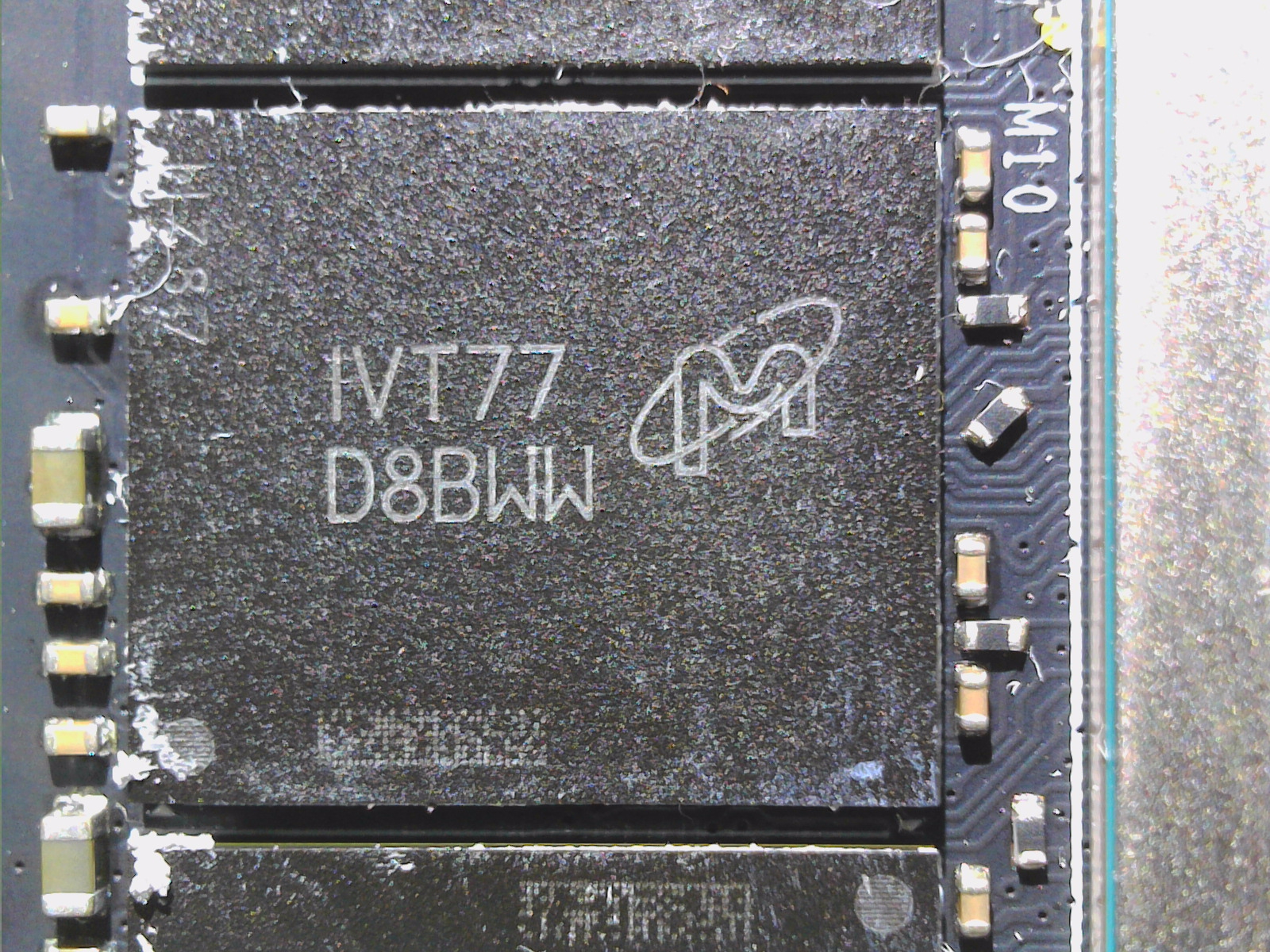
For the memory, KFA2 uses two phases instead of three, which are generated by yet another uP9511R. Here, too, the PLCs are of the same type as the previous ones. However, the PWM controller is on the front The PLC of the PCI Express voltage PEXVDD is on the front and the 1.8 Volt PLC is on the back, the associated coils on the front. There is also a 5V conditioning at the bottom right. However, we do not see any thermal pads on the back here.
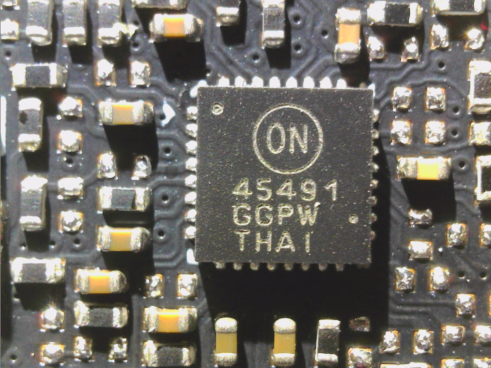
Three coils with 1 µF each are used for input smoothing, behind which a shunt is located. The voltage drop of the shunt is used to measure the flowing currents with two NCP 45491 from OnSemi. But since the firmware can also evaluate the MOSFET DCR of the PLC, shunt mods are no longer so easily possible.
Cooler and disassembly
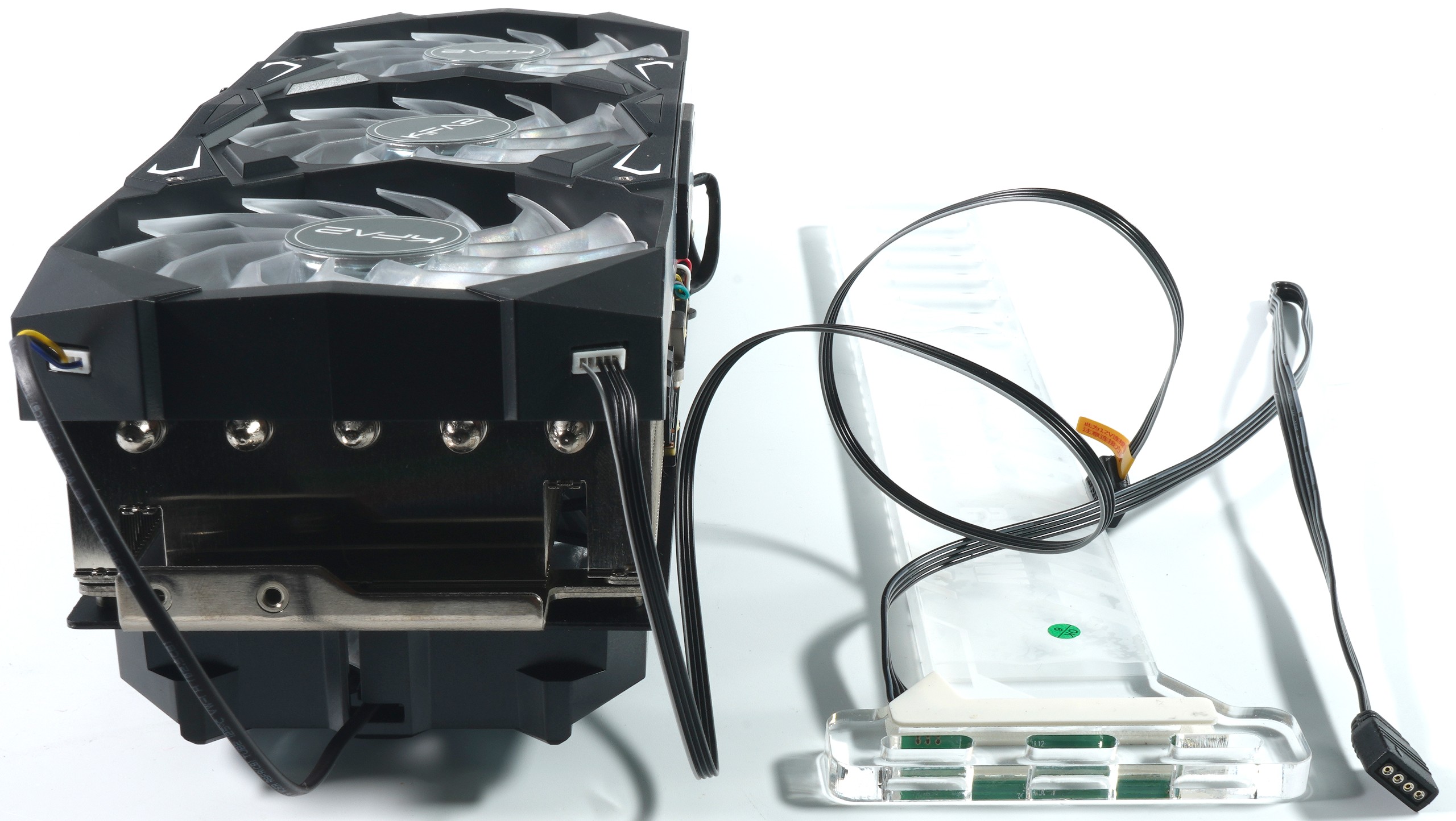
Disassembling the cooler is a bit tricky, although the backplate and most of the screws are easy to remove. The board is quite short, so the third fan is effectively blowing through because the cooler is also open at the back. A total of five thick nickel-plated 6 mm heatpipes made of copper composite material run through the cooler and are pressed in behind the large aluminum heatsink.
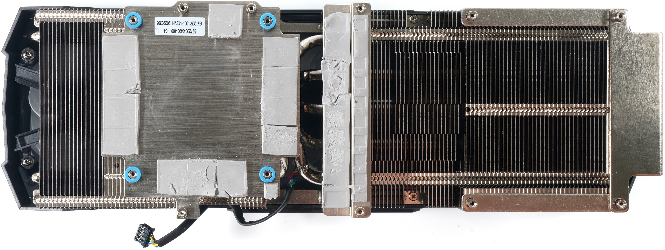
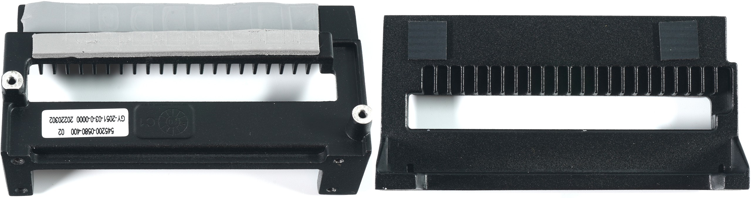
However, what might be a bit of a hindrance to a water cooling conversion is the VRM cooler near the slot bezel. Since this also carries the slot cover via 4 screws, it should no longer hold without the block. Especially since KFA2 uses the block as a counterpart for the M2.5 (5 mm hexagon head) screws, which in turn have another thread in the head for the backplate screw connection and also anchor the lugs of the slot bracket to the PCB.
The backplate is only intended for stabilization and optics, nothing is cooled here.
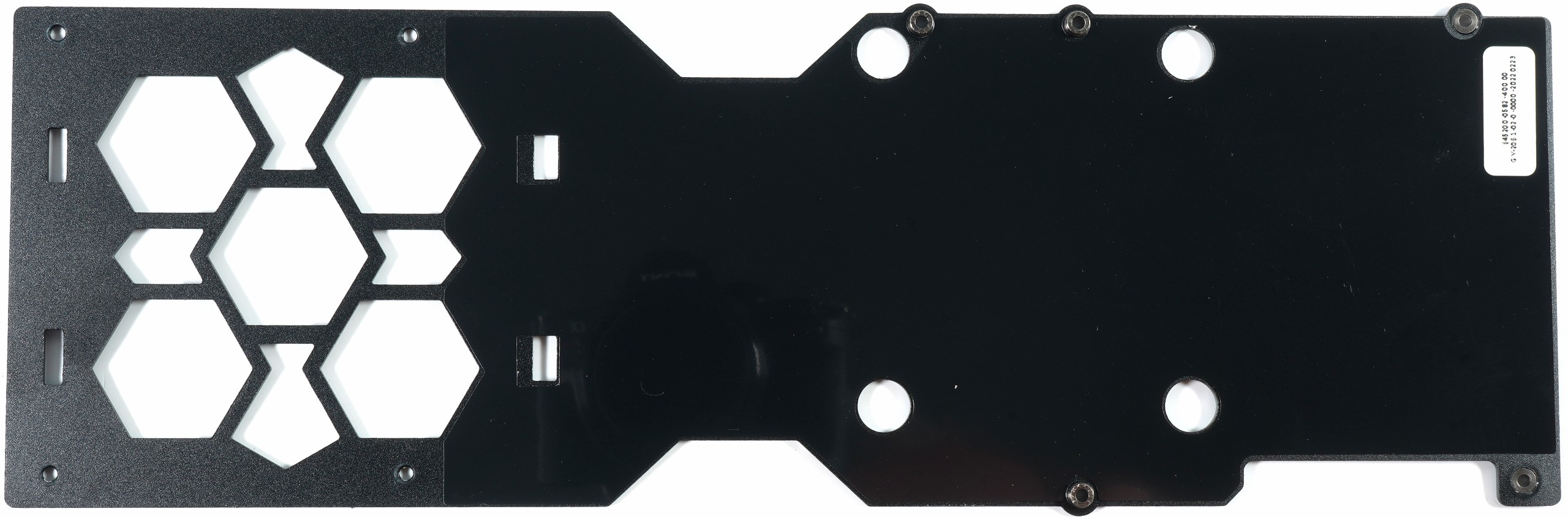
At the end of the card, we can see the connections for the optional rear cooler and the connection of the VGA holder.

- 1 - Introduction, Unboxing and Specs
- 2 - Test System and Methods
- 3 - Teardown: PCB Analysis, Components and Cooler
- 4 - Gaming Performance
- 5 - Gaming Efficiency and Power Draw
- 6 - Power Consumption in Detail and Standards
- 7 - Transients and PSU Recommendation
- 8 - Temperatures and Clock Rates
- 9 - Fan Curve, Fan Speed and "Noise" Analysis
- 10 - Summary and Conclusion


5 Antworten
Kommentar
Lade neue Kommentare
Veteran
Mitglied
Mitglied
Mitglied
Veteran
Alle Kommentare lesen unter igor´sLAB Community →