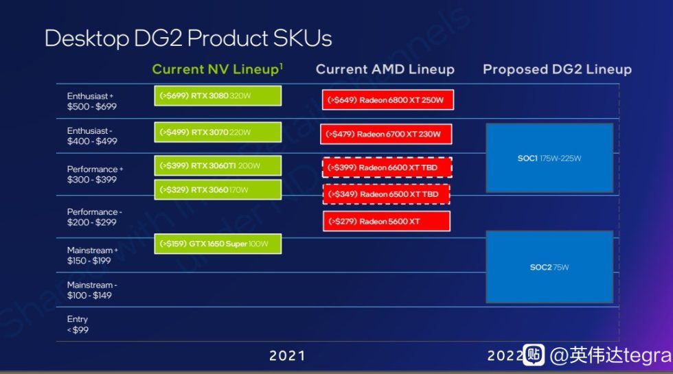
Intel is looking to be in the final stages of bringing the first generation of Arc graphics to market and so it is also obvious to find a nomenclature is the correct order. Because every kid needs his name, even if things like Alchemist aXXX, Battle Mage bXXX and Celestial cXXX do seem a bit thick. But there’s definitely something figurative about it, so marketing be damned.
If you follow @momomo_us’ Twitter post, Intel has created a usage guide of sorts that includes details we didn’t already know, including the fact that the generations will be referred to as Intel Arc aXXX, bXXX, cXXX, and dXXX, respectively. Interestingly, Arc isn’t capitalized as an ARC there either, though marketing usually likes to take it.
Intel Arc a170, a150 and a130 are all possible designations (along with other variants).
🆗Intel® Arc™ a-series graphics
🆖1st Gen Intel® Arc™ graphics pic.twitter.com/pgSNo5avVD— 188号 (@momomo_us) September 26, 2021
The leaked design document mentions that the first generation GPUs are referred to as both Intel Arc a-series and Intel Arc a-series graphics, rather than 1st Generation Intel Arc graphics. Now the nomenclature has been worked out, but with Intel planning exactly three SKUs, we can make some educated guesses as to what the naming scheme might look like.

The first iteration of the Intel Xe HPG GPU will thus have 8 so-called slices, each consisting of 4 Xe cores. This gives a total number of 512 vectors/matrices (8x4x16). This is exactly what the older “EU” (Execute Units) count of this GPU was. Assuming that the base architecture is the same (which it should be), we are thus still dealing with 4096 execution units buw. Cores (512*8).
The Intel Xe HPG are manufactured in the 6nm process by TSMC, which should already give a real kick in terms of energy efficiency and transistor density. Incidentally, this also means that you could see decent unit sales at launch if the Node delivers what it promises. Intel’s Xe HPG architecture will then certainly be able to achieve clock rates up to 1.5 times higher than Xe LP and thus also deliver up to 1.5 times more performance per watt. This means that one could expect clock rates in the range of 2.1 GHz, while the first discrete Xe LP GPUs were still clocked with a rather meager 1.4 GHz (see also our first tests with the DG1).

We will have to wait for more information or leaks to round out the final picture even better – so it remains exciting.
Source : momomo_us


5 Antworten
Kommentar
Lade neue Kommentare
Urgestein
Urgestein
Urgestein
Urgestein
Urgestein
Alle Kommentare lesen unter igor´sLAB Community →