


Update from 24/04/2019 at 09.30
In the meantime I have also been able to insert all chart graphics. A total of 12 additional pages, also with single graphics for all tested maps, have been added. I will now add the rest in real time. Also the conclusion, which above all reflects why Nvidia probably made such a tin top because of the drivers. But even this is best done by yourself and then looks at the conclusion. I would like to leave the opinion-forming to our readers first.
Original article
One would almost like to think that the GeForce GTX 1650 is a bit like Nvidia's unloved child, because it is hard to explain the withholding of the (long-finished) drivers until the launch day. This is a pity, because it is hardly possible to get clean and objective tests at the launch date. The fact that I can still publish something today and the rest will hopefully appear tomorrow in the form of further benchmarks is also due to the DIY mode of the editor, who once again sees the whole thing as a personal challenge. In the meantime, however, everything has also been benchmarked and supplemented here in the article!
I first created today's tests with an unofficial driver that I had crafted myself from an older game-ready and an evaluation driver. For all things, such as the operation of the card in various load scenarios for the power consumption and thermal measurements, as well as the acoustic measurements, this solution is completely sufficient. But I also want to remain fair and objective, not to benchmark the entire parkour with it. It is and remains not an official driver (even if it is not yet running) and so I only use my own creation for the most important laboratory tests. That's why all games had to be reworked. But now everything is complete.
Plausibility tests with the evaluation driver have shown that even in the few applications supported at all, its performance is still well below what could have been predicted purely mathematically. All the results published with it are definitely false and unusable. And it is also the journalist's responsibility not to use his own driver creations to publish their results as objective results. Then we'd rather wait a day and that's exactly what we did.
In my recent article Green Easter Egg? What we already know about the GeForce GTX 1650 (and what not) I had already speculated (correctly) and calculated what the TU117-300 called chip could and couldn't do. And it's a pity once again that Nvidia treats the new GeForce entry-level class so poorly. Because these cards are not only intended for the mostly anonymous system integrators and ready-made PC manufacturers, but also for the mostly young and not quite as cash-rich clientele.
I wrote it that often enough with the first "real" graphics card for small money, a later brand loyalty is established and the customer is shaped. That's why the board partners are certainly not so happy with the renewed lack of respect, which surprised us even then with the GeForce GTX 1050 Ti. But what is it, because Nvidia at least achieves that if they keep something on their hands, the editors will again be present with two articles on one product and will push the gaming results after the allocation of the final drivers. The writing guild is so predictable…
The TU117-300 is not a real full-end
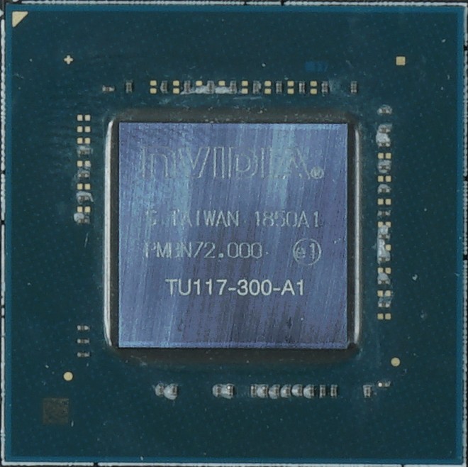 Well, let's see what Nvidia offers us here. By the way, the chip dates back to December last year, so the GeForce GTX 1650 isn't so fresh. But we come to the inner workings and the construction of the TU117-300. While Turing's streaming multiprocessors consist of fewer CUDA cores than Pascal's, the design compensates for this in part by distributing more streaming multiprocessors (SM) on the GPU.
The Turing architecture assigns each set of 16 CUDA cores, one scheduler, and one disposition unit per 16 CUDA cores (such as Pascal). Four of these 16-core groupings include the SM, 96 KB cache, which can be configured as 64 KB L1/32 KB of shared memory, or vice versa, and four texture units. As a result, the TU117-300 of the GeForce GTX 1650 with its 896 CUDA cores has such 14 SM. If you followed Nvidia's nomenclature for the chip designation, a larger TU117-400 would only be logical.
But the theory also confirms the fact that the TU117-300 is not the maximum expansion. I have modified and shortened a scheme of the TU116-300 of the GeForce GTX 1660 to fit exactly for the TU117-300 of the GeForce GTX 1650. We see very nicely the gaps in the two GPC, so that the TU117-400, if it will exist, could appear with 16 SM, which should also run out as a result of 1024 CUDA-Cores. Unfortunately, Nvidia does not reveal whether this could be a GeForce GTX 1650 ("We generally don't talk about unannounced products").
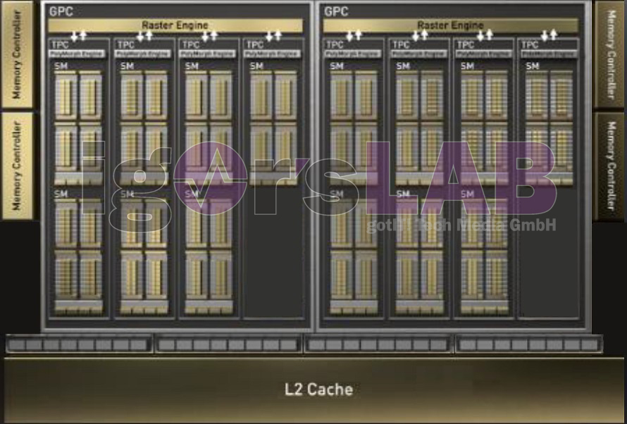
Because Turing has twice as many schedulers as Pascal, only one statement needs to be issued to the CUDA cores in every second cycle. In between, there is enough room to send a different instruction to any other device, including the INT32 cores. This is no different with the GTX 1650 than with the other larger Turing cards. Nvidia splits these 14 SM into two graphics processing clusters. In addition, 14 SMs, each with four associated texture units, total56 texture units for the entire GPU.
In addition to the Shaders and the Unified Cache of the Turing Architecture, the TU117 also supports a pair of algorithms called Content Adaptive Shading and Motion Adaptive Shading, which together are called variable-rate shading. I have already written a longer introduction to the launch of the GeForce RTX 2080 (Ti). Nvidia has also revealed that it is replacing the tensor cores with dedicated FP16 cores to enable the GeForce GTX 1660 Ti to process semi-precision operations at twice the rate of FP32. Nvidia has also noted that the TU117 is the smallest Turing chip that will be able to use the DXR share in the drivers.
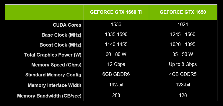
Four 32-bit memory controllers end up giving the TU117 an aggregated 128-bit bus that operates the four GDDR5 modules at up to 128 GB/s. However, this is a considerable bandwidth disadvantage compared to the GTX 1660 and is even lower than the level of the old GeForce GTX 1060, but also significantly higher than that of the GeForce GTX 1050 Ti.
The following table shows the relevant models and a fictitious GeForce GTX 1650 Ti:
| Nvidia GeForce GTX 1060 |
Nvidia GeForce GTX 1660 Ti 6 GB |
Nvidia GeForce GTX 1660 6 GB |
Nvidia GeForce GTX 1650 |
Msi GeForce GTX 1650 Ti Gaming X |
Nvidia GeForce GTX 1650 Ti |
|
| Architecture (GPU) |
GP106 | TU116-400 | TU116-300 | TU-117-300 | TU-117-300 | TU117-400 |
| CUDA Cores |
1280 | 1536* | 1280* | 896 | 896 | 1024 |
| Tensor Cores |
No | No | No | No | No | No |
| RT Cores |
No | No | No | No | No | No |
| Texture Units |
180 | 96 | 80 | 56 | 56 | 64 |
| Base Clock Rate |
1506 MHz | 1500 MHz | 1530 MHz | 1485 MHz | 1485 | ? |
| GPU Boost Rate |
1708 MHz | 1770 MHz | 1785 MHZ | 1665 MHz | 1860 | ? |
| Storage expansion |
6 GB GDDR5 | 6 GB GDDR6 | 6 GB GDDR5 | 4GB GDDR5 | 4GB GDDR5 | 4GB GDDR5 |
| Storage bus |
192-bit | 192-bit | 192-bit | 128-bit | 128-bit | 128-bit |
| Memory clock |
4000 MHz | 6000 MHz | 4000 MHz | 4000 MHz | 4000 MHz |
4000 MHz |
| Rops |
48 | 48 | 48 | 32 | 32 | 32 |
| L2 Cache |
1.5 MB | 1.5 MB | 1.5 MB | 1 MB | 1 MB | 1 MB |
| Board design | PG161 | PG165 | PG174 | Custom | PG174 | |
| Tdp |
120 W | 120 W | 120 W | 75 W | 85 W | ? |
| Transistors |
4.4 billion | 6.6 billion | 6.6 billion | 4.7 billion | 4.7 billion | 4.7 billion |
| The size |
200 mm2 | 284 mm2 | 284 mm" | ? | ? | ? |
| Sli |
No | No | No | No | No | No |
Incidentally, Nvidia is also launching the notebook varinates of two GPUs today, which I would like to include at least as a data overview:
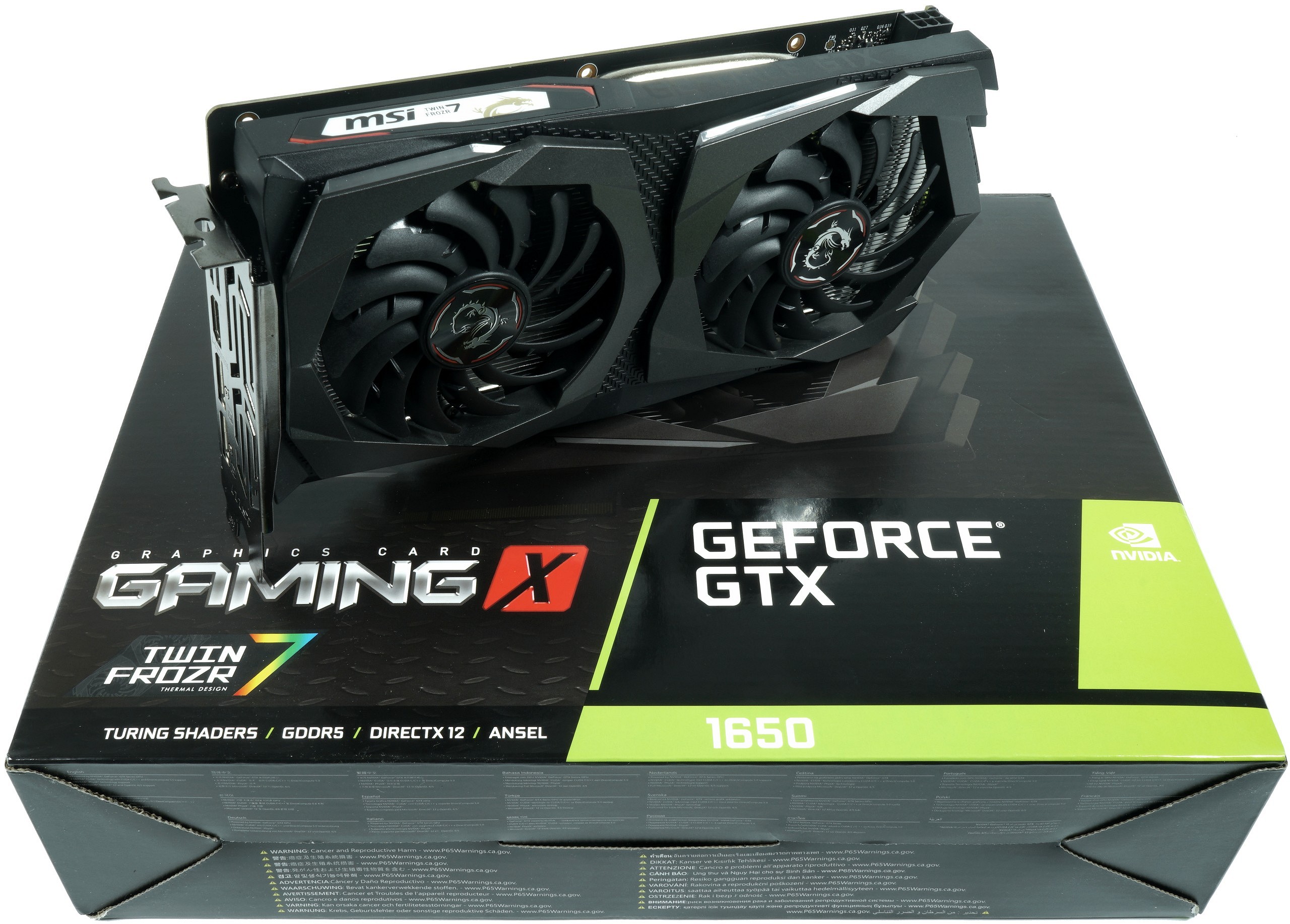
The MSI GeForce GTX 1650 Gaming X
There is again no reference card from Nvidia, so the launch goes directly to the board partners this time. For my test, I picked out the MSI GTX 1650 Gaming X as the main card, even if this time the actual clock rate for all tested cards is more or less the same at the end. But the effort for teardown and board analysis is simply too high for two or even three such cards at the end, so I ask for your understanding. The US editorial team tested a map of gigabytes, which unfortunately could not (or did not want to be) available to us here, but which performs similarly.
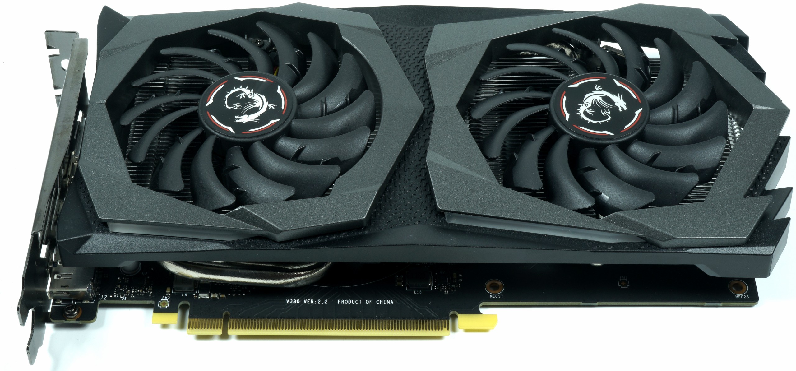
The 576-gram card measures 24.5 cm gross in length from the outer edge slot bezel to the end of the radiator cover. It is 3.6 cm thick and 12 cm high (from the top of the motherboard slot to the top edge of the radiator cover). The anthracite-coloured radiator cover is kept in the usual MSI-Edge style and quite restrained. It only gets a little brighter with electricity, because you can find at least the MSI logo on the top as a foil, behind which hangs a monochrome LED.
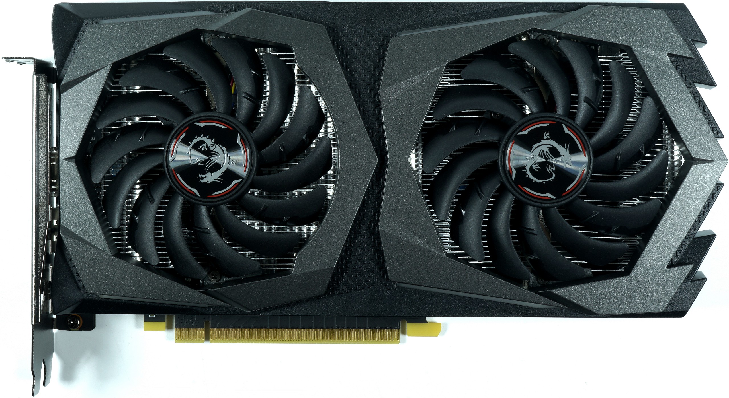
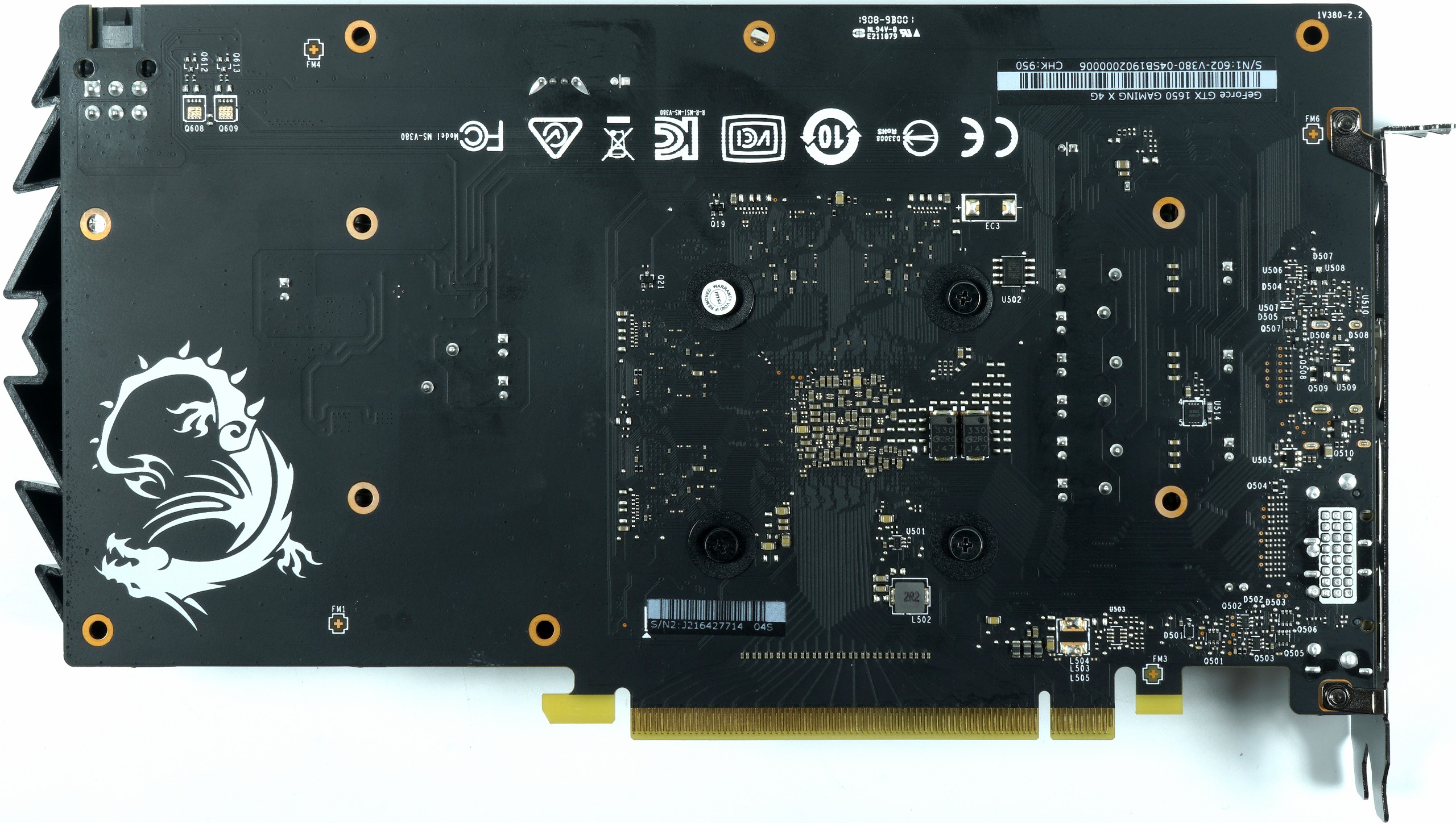
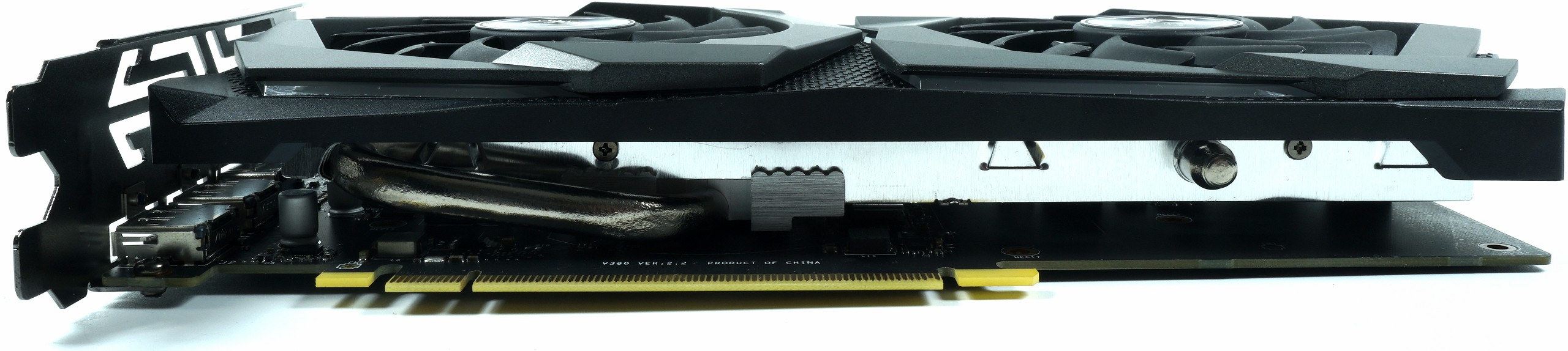
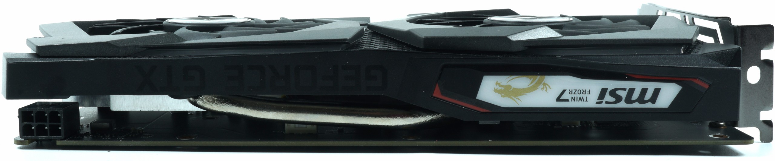
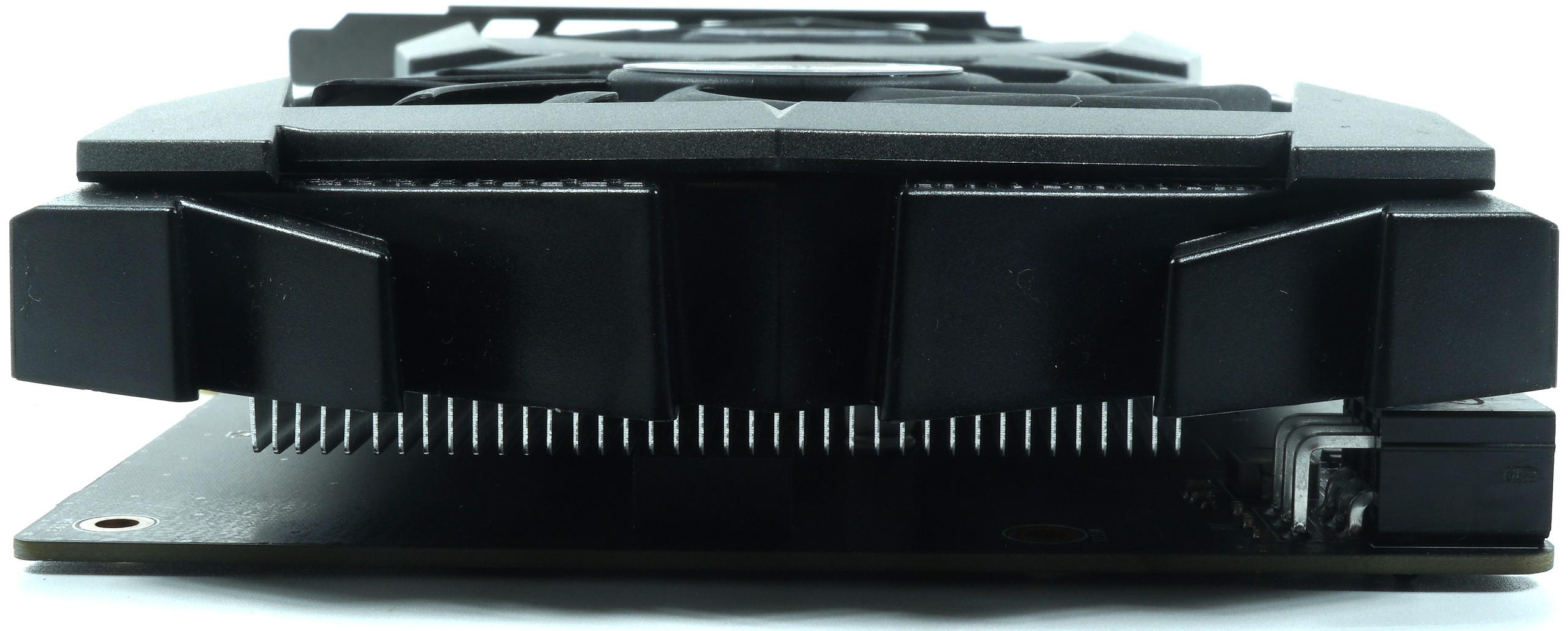
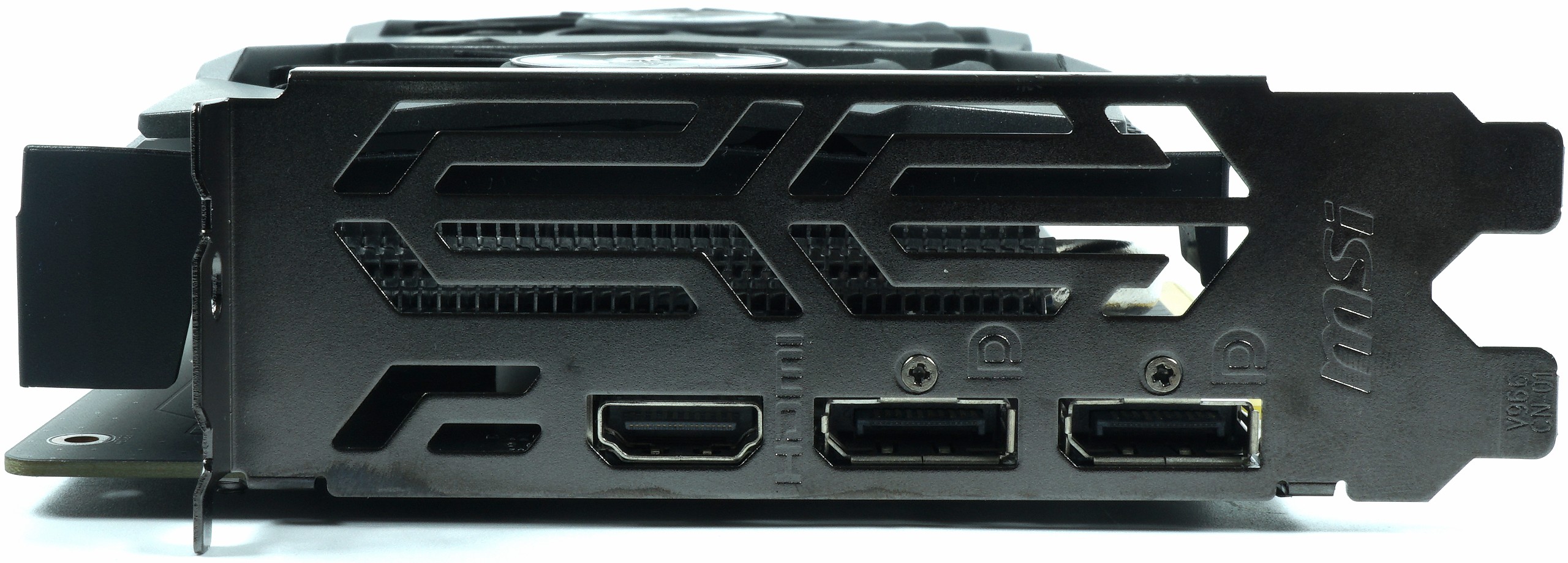
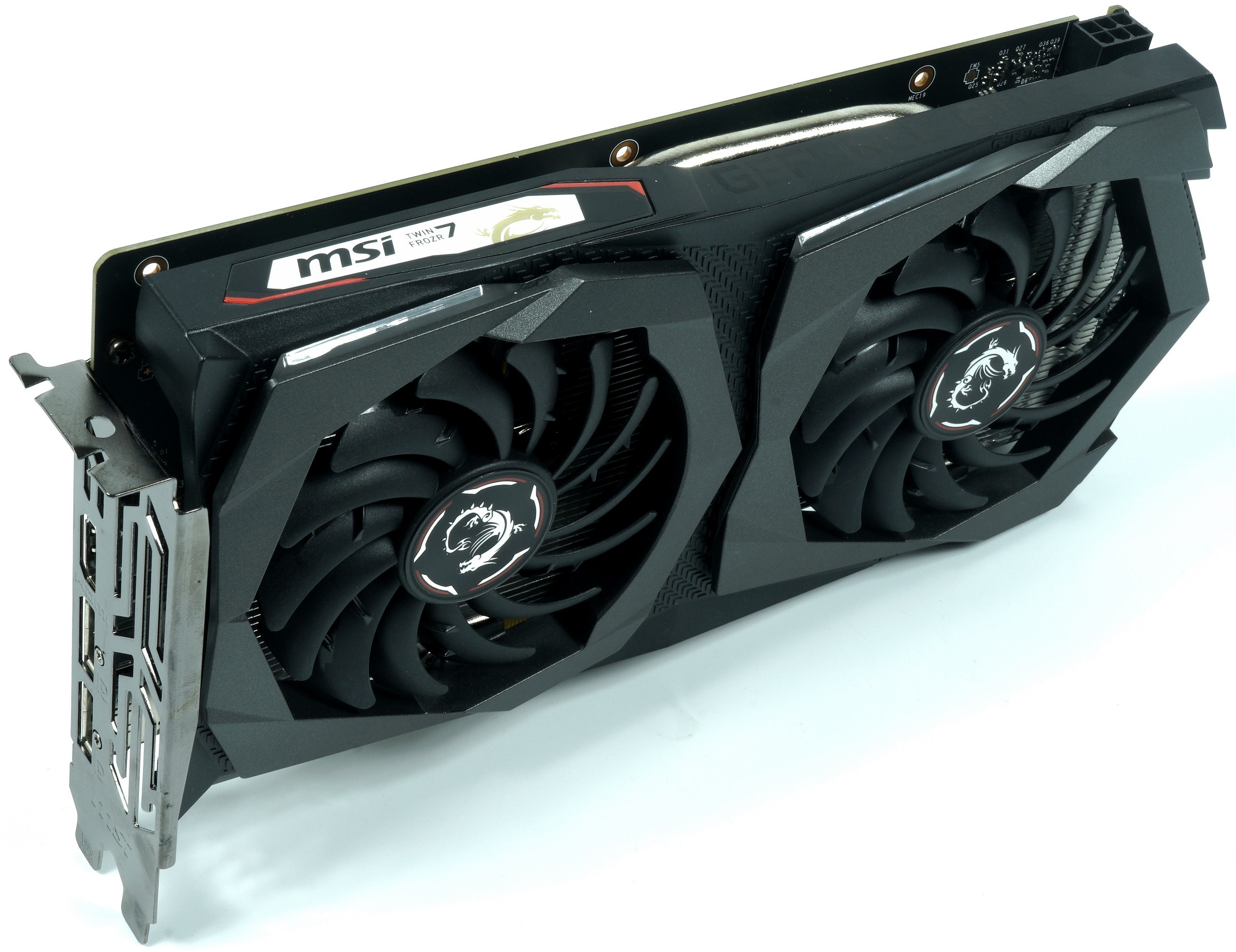

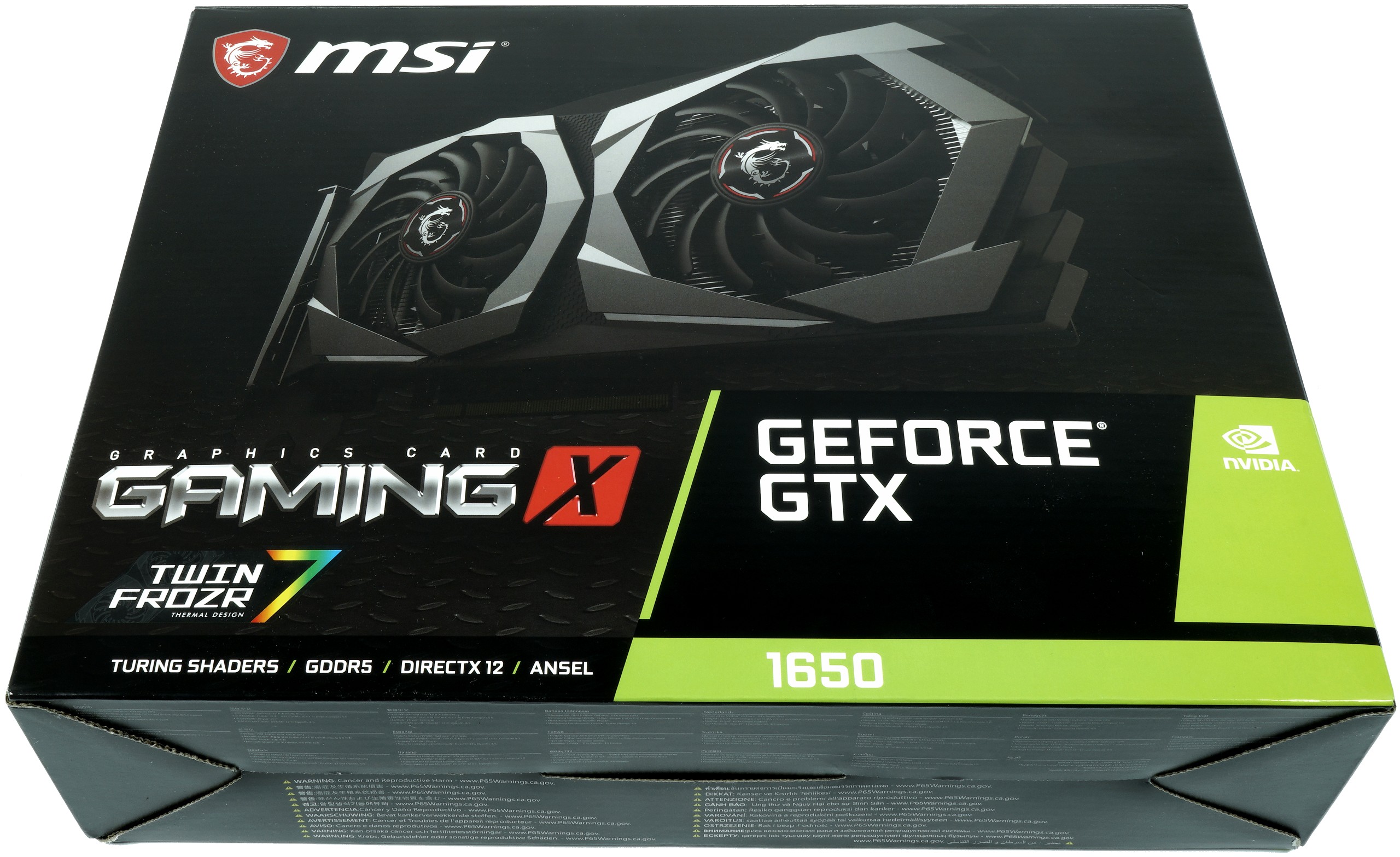
The two 8.5 cm fans with their 14 rotor blades are almost lost on this card. Of course, a backplate can no longer be found in this price range and so MSI has at least had the dragon logo printed on a free space of the board. Because there's enough of that. A simple 6-pin power supply connection at the top must be enough, but it does. The connection cost is even leaner, because in addition to the one HDMI 2.0 connection you will find two DisplayPort connections. That's it.
Test system and measurement methods
I have already described the new test system and the methodology in the basic article "How we test graphics cards, as of February 2017" (English: "How We Test Graphics Cards") in great detail and therefore, for the sake of simplicity, now only refers to this detailed Description. So if you want to read everything again, you are welcome to do so.
If you are interested, the summary in table form quickly provides a brief overview:
| Test systems and measuring rooms | |
|---|---|
| Hardware: |
Intel Core i7-7700K (analogous to TH US) MSI Z270 Gaming Pro Carbon AC 16GB KFA2 DDR4 4000 Hall Of Fame @DDR4 3200 1x 1 TByte Toshiba OCZ RD400 (M.2, System SSD) 2x 960 GByte Toshiba OCZ TR150 (Storage, Images) Be Quiet Dark Power Pro 11, 850-watt power supply |
| Cooling: |
Alphacool Ice Block XPX 5x Be Quiet! Silent Wings 3 PWM (Closed Case Simulation) Thermal Grizzly Kryonaut (for cooler change) |
| Housing: |
Lian Li PC-T70 with expansion kit and modifications Modes: Open Benchtable, Closed Case |
| Monitor: | Eizo EV3237-BK |
| Power consumption: |
non-contact DC measurement on the PCIe slot (Riser-Card) non-contact DC measurement on the external PCIe power supply Direct voltage measurement on the respective feeders and on the power supply 2x Rohde & Schwarz HMO 3054, 500 MHz multi-channel oscillograph with memory function 4x Rohde & Schwarz HZO50, current togor adapter (1 mA to 30 A, 100 KHz, DC) 4x Rohde & Schwarz HZ355, touch divider (10:1, 500 MHz) 1x Rohde & Schwarz HMC 8012, digital multimeter with storage function |
| Thermography: |
Optris PI640, infrared camera PI Connect evaluation software with profiles |
| Acoustics: |
NTI Audio M2211 (with calibration file) Steinberg UR12 (with phantom power for the microphones) Creative X7, Smaart v.7 own low-reflection measuring room, 3.5 x 1.8 x 2.2 m (LxTxH) Axial measurements, perpendicular to the center of the sound source(s), measuring distance 50 cm Noise in dBA (Slow) as RTA measurement Frequency spectrum as a graph |
| Operating system | Windows 10 Pro (1809, all updates) |
- 1 - Einführung, Unboxing, Chip-Details und Testsystem
- 2 - Tear Down: Platinen- und Kühleranalyse
- 3 - Ashes of the Singularity
- 4 - Battlefield V
- 5 - Destiny 2
- 6 - The Division 2
- 7 - Far Cry 5
- 8 - Forza Horizon 4
- 9 - Ghost Recon
- 10 - Grand Theft Auto V
- 11 - Metro Last Light
- 12 - Shadow of the Tomb Raider
- 13 - The Witcher 3
- 14 - Wolfenstein II
- 15 - Leistungsaufnahme und Netzteilempfehlung
- 16 - OC, Taktraten, Temperatur, Infrarot
- 17 - Lüfter und Lautstärke
- 18 - Zusammenfassung und Fazit


Kommentieren