Intel wants and needs to set with Alder Lake as 12th generation a big mark in the mainstream market for desktop CPUs this year, if they don’t want to lose the connection (also from their target group’s point of view). And it is not only a repainted and further upgraded 14 nm CPU, but in addition to the smaller structure width of 10 nm (according to Intel’s reading), it is finally also a completely new architecture with a completely different solution approach. Can certainly work out, but the outcome is a bit uncertain, at least for now, looking at AMD’s Warhol. Now, however, an engineering sample (ES) of an Intel Core-1800 has surfaced, which already tells me and thus us a bit more in so many respects.
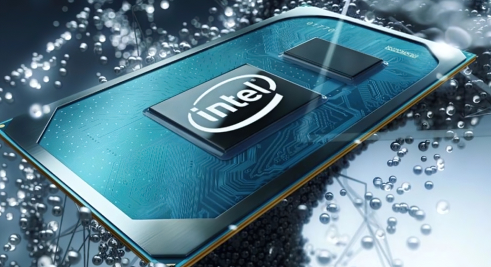
But what are Intel’s plans? For the first time, the Big Little approach, which has already been used for many years in the ARM SoCs of mobile devices such as smartphones and tablets, is being used. The principle is actually as simple as it is efficient, because large and small processing cores cleverly divide the work between themselves, depending on the load. The less demanding tasks are outsourced to power-saving, small Atom cores, while the larger cores are then assigned the more computationally intensive tasks and are of course allowed to consume more power in return. This is all already known.
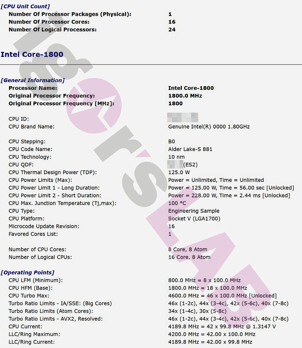
In the ES of the Core-1800 in the (not final) B0-stepping presented today, there are 8 large Golden Cove cores (Core) and 8 small Gracemont cores (Atom) on the die. While the big cores are also capable of hyperthreading, this is not the case with the Atom cores. In total, you’ll find 16 cores that can process a maximum of 24 threads. According to various leaks, Intel quantifies the performance leap compared to a conventional solution (unfortunately not specified) with up to 20 percent in pure single-thread scenarios and a doubling of the multi-thread performance in the ideal case, which seems quite optimistic when you consider a current 8-core of the 11th generation.
The processor, internally called Intel Core-1800, sits in the new Socket V (LGA 1700) and has a TDP of 125 watts. The screenshot below, which I modified slightly to protect the source, shows a time of 56 seconds for the PL1 and a peak time of 2.44 ms for the PL2 of a whopping 228 watts. That this up- and down-switching is well suited to aggravate the already nervous load change behavior of the current Intel CPUs even more doesn’t even have to be mentioned. This is where the voltage converters of the mainboards come into play.
The revision B0 of this ES is still quite early and the base clock is also still quite low with only 1800 MHz. More interesting are the Turbo Boost limits of the big cores, where 1-2 cores are already supposed to reach 4.6 GHz, with 3-4 cores it’s still 4.4 GHz, with 5-6 cores 4.2 GHz and with all 8 cores then 4 GHz. The small Atom cores clock with up to 3.4 GHz with <=4 used cores, otherwise only with 3 GHz. The image above also shows a voltage value that Intel locates at 1.3147 V. The rest is self-explanatory.
According to the initial information, the new desktop CPUs will support up to dual-channel DDR5-4800 memory and the DDR4-enabled motherboards will support modules up to 3200-MHz. Supposedly, only the high-end Z690 motherboards will offer DDR5 support, while all cheaper variants will still rely on DDR4. This would then give Intel and also the motherboard manufacturers much more flexibility and security when it comes to the still unclear DDR5 mass production.
Another big upgrade coming with Alder Lake-S is support for PCIe Gen5. The CPU will have 16 PCIe Gen5 capable lanes and in addition 4 lanes in PCIe Gen4 standard. The 600 chipset itself will then support Gen4 and even still Gen3. In addition, the Direct Media Interface (DMI) has been upgraded to Gen4. If there is any further information, I will of course not withhold it from you.










63 Antworten
Kommentar
Lade neue Kommentare
Mitglied
Urgestein
Mitglied
Mitglied
Mitglied
Mitglied
Urgestein
Veteran
Veteran
Urgestein
Urgestein
Veteran
Urgestein
Mitglied
Urgestein
Mitglied
Veteran
Urgestein
Mitglied
Alle Kommentare lesen unter igor´sLAB Community →