


I had already reported a few things about NVIDIA’s new generation of Ampere cards in several articles and read the feedback on them. Interesting there were especially the extrapolations of the number of possible CUDA cores, where all comparisons to Turing regarding performance and efficiency and as a consequence also with the possible power consumption were made. Or better: you believe you can attach it to it. However, the sole scaling of the CUDA cores as the scale of an estimateis a real problem, which I would like to explain.
Important preliminary remark
Today’s article is a pure thought experiment, based on many tests with the Quadro RTX 6000, 5000 and 4000 in the workstation area and many bottlenecks that have appeared when sharing from the CUDA cores to the RT and Tensor cores. The measurements and comparison data certainly suggest a certain dilemma resulting from NVIDIA’s self-imposed fixed power limit and the way Boost, with its up and down, ultimately also indirectly affects Tensor and RT performance. This is not always equal and balanced.
What I’m getting at and why, we might finally see a much more efficient solution for the power supply, you could read in the following article, which is not a leak, but is based on many facts, which you just have to recognize, collect and put together. Nevertheless, I would like to explicitly state in advance that it is only my view of things and that everything could turn out a bit different in the end. Anyway
Approach
What I’m getting at is that many people may have noticed that Nvidia has been focusing more and more (and almost aggressively) on the topic of AI and especially local DLSS (Deep Learning Super Sampling). And not only for the gamers, but also on a broad front in the productive area. It is certainly no secret that, in addition to the RT cores, the tensor cores play a significant role here. What amazes me, however, is the fact that with all the leaks and estimates, it’s all about the classic shaders and you simply leave aside what RTX is all about.
For “Big Navi” you can expect quite a lot of performance from AMD, and it’s not without reason that the GA102 will already be in the game on the launch day as a full version. The RT performance of the AMD card is hard to estimate, but even here some things will probably be possible. What “Big Navi” is obviously still missing, however, are the specialized Tensor Cores, which play a not insignificant role for AI and meanwhile also countless use cases in productive programs. And that’s exactly where it gets interesting, because why should Nvidia neglect the only really exclusive field in comparison to its direct competitor? Ray tracing was already presented at the time and I would be very much mistaken if I didn’t focus more on the Tensor performance.
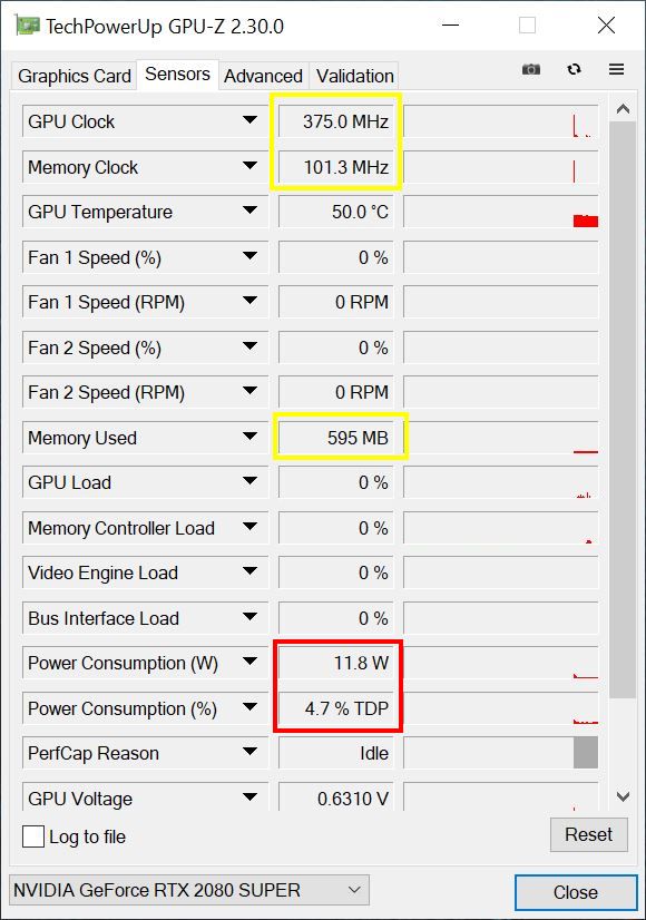
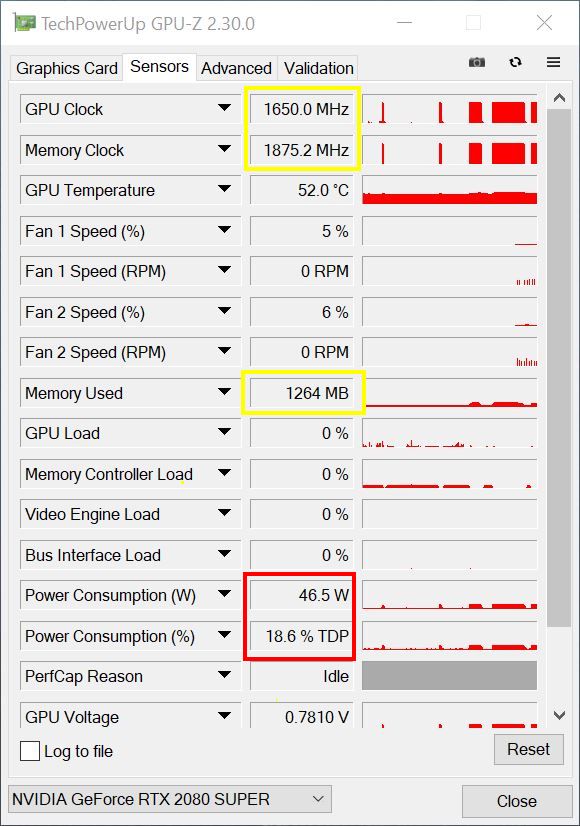
However, if the share of tensor cores in the energy supply concept were to be significantly increased, one would suddenly be faced with a real problem. Do you remember my test on RTX Voice and the comparison between CUDA and Tensor cores? Who ever was looking for a test on how to reduce the load or can determine the power consumption of the Tensor cores: in idle this is even possible with RTX Voice, because there is no graphics load. By the way, a similar effect can always be observed when, for example in various filters, the image processing or video editing program uses these specialized cores. Power consumption high, GPU load supposedly at zero.
The bottleneck of the power supply at Turing
Now let’s look at Turing’s power supply scheme for the first generation RTX. To understand the following, I must first return to important basics. Because we now need to be clear about the term Total Graphics Power (TGP). It’s still quite easy to measure this on all feeders, but what makes NVIDIA and AMD completely different is the control and regulation rage on NVIDIA’s current graphics cards, where the respective power target (default power limit, factory default) and the maximum power limit (max power limit, absolute value) are fixed in the firmware.
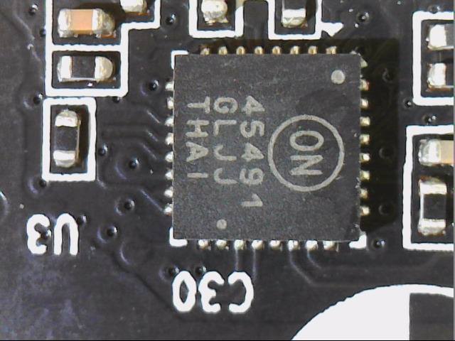
We see for the GeForce RTX 2080 Ti e.g. 13 voltage converter circuits for VDDC, distributed over 8 phases. In addition there are 3 phases for the memory (MVDD) and a lot of small partial voltages, which are not very important as items.
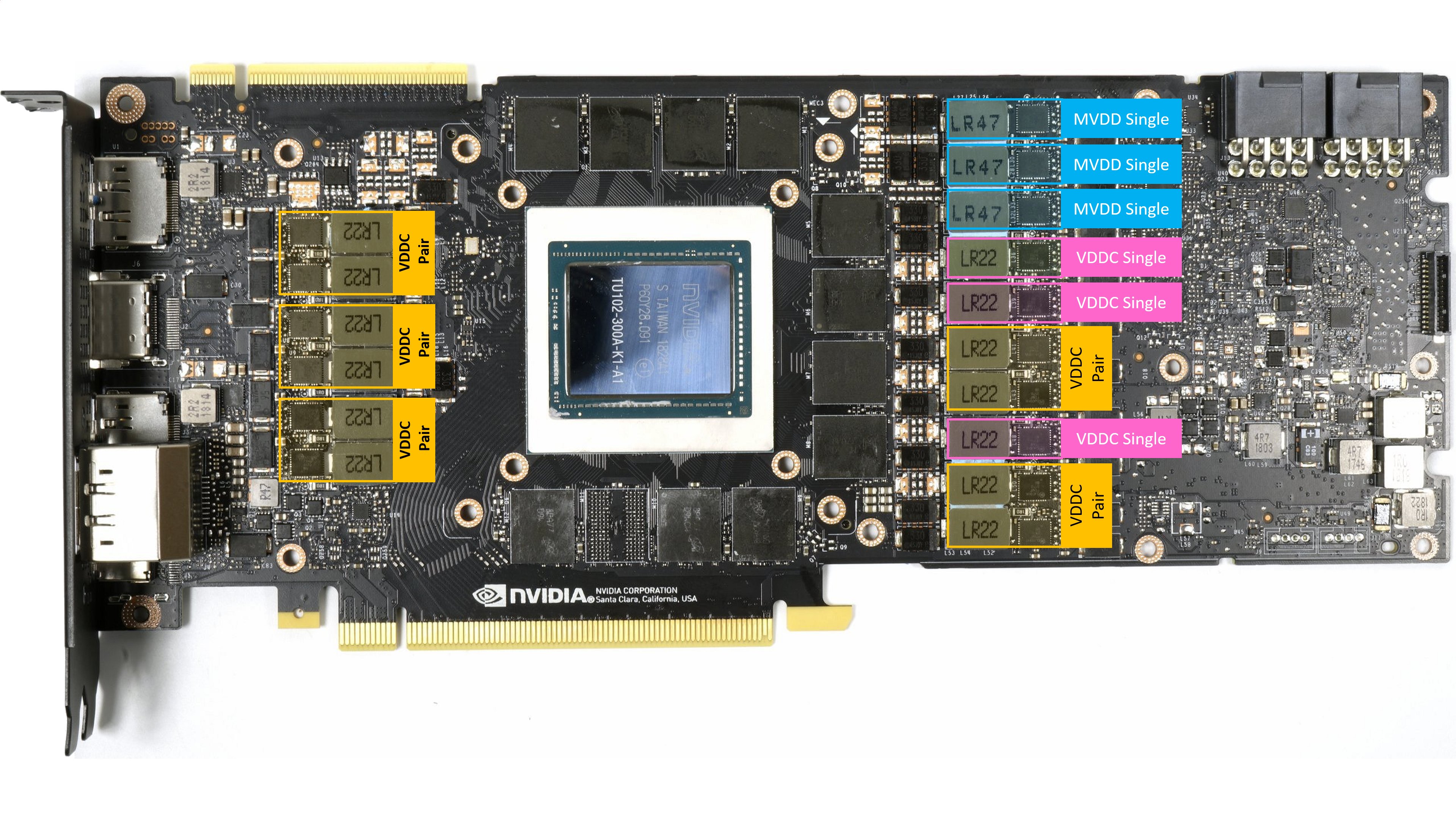
In contrast to AMD, Nvidia meticulously monitors all 12-volt inputs using a special monitoring chip, which measures the voltage behind and in front of the shunt (very low resistance) and thus also evaluates the voltage drop across this shunt (from which the current flow is calculated). Since there is such a shunt in every 12 Volt supply line, the exact power consumption of the board at 12 Volt can be measured and used as a basis for the internal limitation of the power consumption. On the left we see a shunt with a longitudinal coil for input smoothing and on the right a NCP45491 from On Semi for monitoring voltages and currents.

Exactly this value determined here is never (can never be) exceeded in practice, this is ensured by the very attentive and fast regulating firmware. What many people don’t consider is that this calculation also includes fans, RGB floodlight, microcontrollers and displays. The more “peripherals” have to be supplied, the less power is available to the GPU! 35 to 45 watts, which can be with the RTX 2080 Ti for the maximum load of the Tensor and RT cores could estimate, not so restrictively in the monitoring included, the cards could profit with full load on CUDA, Tensor and RT cores naturally more clearly!
Unfortunately, the power supply of the two other core units (RT and Tensor) is done via a common line (VDDC) together with the CUDA cores and is also behind the monitored feeds. And the supply voltage also fluctuates and is subject to the control rage of Boost. Which finally closes the circle in the thought process and even the last one realizes that a new solution is actually more than overdue.
What if? How to explain and divide up the 350 watts that are circulated
Up to now, the Turing GPU is supplied with a single voltage for everything, namely VDDC, in addition to the other partial voltages, which have a lower overall weight. Well, I had already mentioned in older publications that you can get a TGP of up to 350 watts for the big SKU10 (I deliberately avoid a name that will surely change anyway) and a TGP of 320 watts for the SKU20 and SKU30. According to my first estimate, this would result in about 230 watts for the entire chip including the CUDA, RT and Tensor cores
| SKU 10 | Estimated Power Consumption / Losses |
| Total Graphics Power TGP | 350 watts |
| 24 GB GDDR6X memory (2.5 Watts per module) | -60 watts |
| MOSFET, Inductor, Caps GPU Voltage | -26 watts |
| MOSFET, Inductor, Caps Framebuffer Voltage | -6 watts |
| MOSFET, Inductor, Caps PCIExpress Voltage | -2 watts |
| Other Voltages, Input Section (AUX) | -4 watts |
| Fans, Other Power | -7 watts |
| PCB Losses | -15 watts |
| GPU power | approx. 230 Watts |
I’m pretty sure that Nvidia will increase the Tensor and certainly the RT performance significantly. Despite the finer node, the power consumption values for these cores should (slightly) increase if a significant difference is to be seen. This can no longer be solved in a meaningful way using a common power supply for all three areas. And even if that were the case, a much more intelligent balancing would have to be achieved.
I think that 60 to 70 watts is the minimum that can be used for the additional core units in the GA102 full configuration, and if the whole thing is decoupled from the CUDA cores, then the power supply can be made a little simpler there as well. In a previous calculation I had used 16 voltage converter circuits for pure GPU power at 230 watts. In addition, up to 4 additional control loops would be required for the memory, at least with a full 24 GB configuration.
Of course, you can also use the calculator and data sheet to make an estimate of how the possible distribution of the GPU voltages could look like. Two times 8 control loops would be quite pointless, because they would not correspond to the power share. The largest PWM controller available at normal prices currently generates a maximum of 10 phases. With a bit of imagination (and luck in guessing), you could set the supply of the shaders with up to 10 phases, whereby each phase would then only address one power stage. The remaining up to 6 phases were then allocated to another partial voltage with the same power stage distribution.
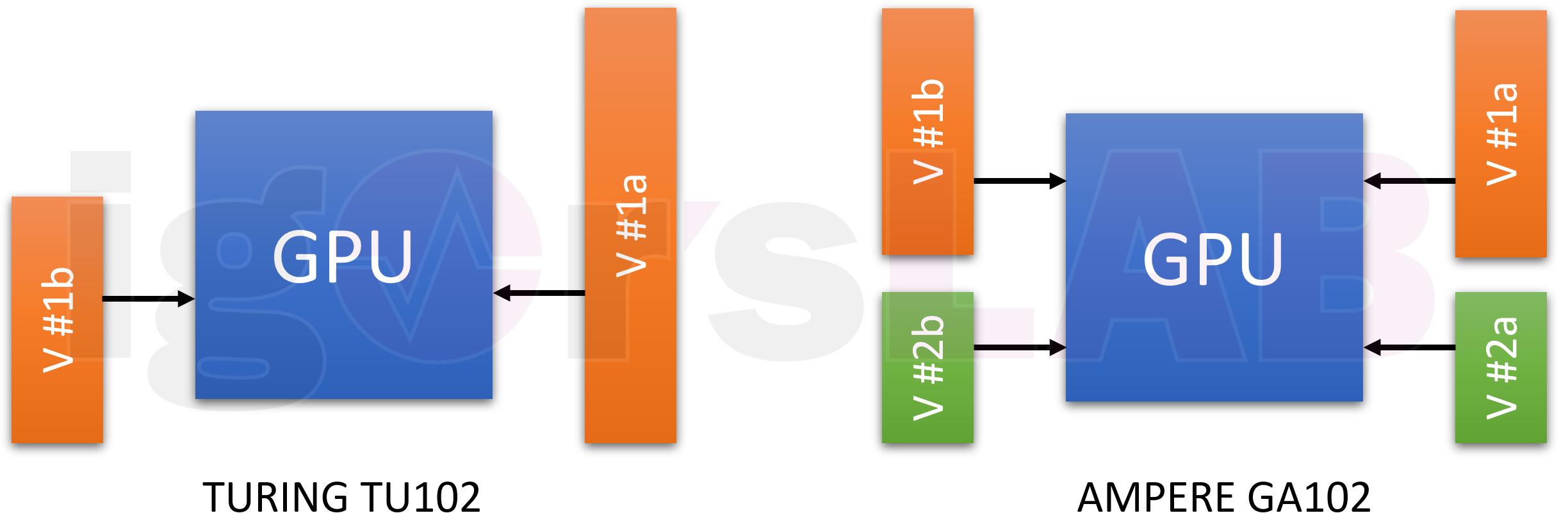
If you calculate this further, the shaders would only have a maximum of 160 to 170 watts, which would make the ratio between Turing and ampere more realistic again. In the case of notebooks, for example, Dynamic Boost is used, where the power distribution is shifted as required in order to remain within the thermal and power limits. A smart balancing between the possible two partial voltages, where the tensor and RT cores would be weighted at least equally, would actually be only logical.
As already written, these are pure mind games. But it would be smart if the actual solution would look like this or at least similar.


Kommentieren