


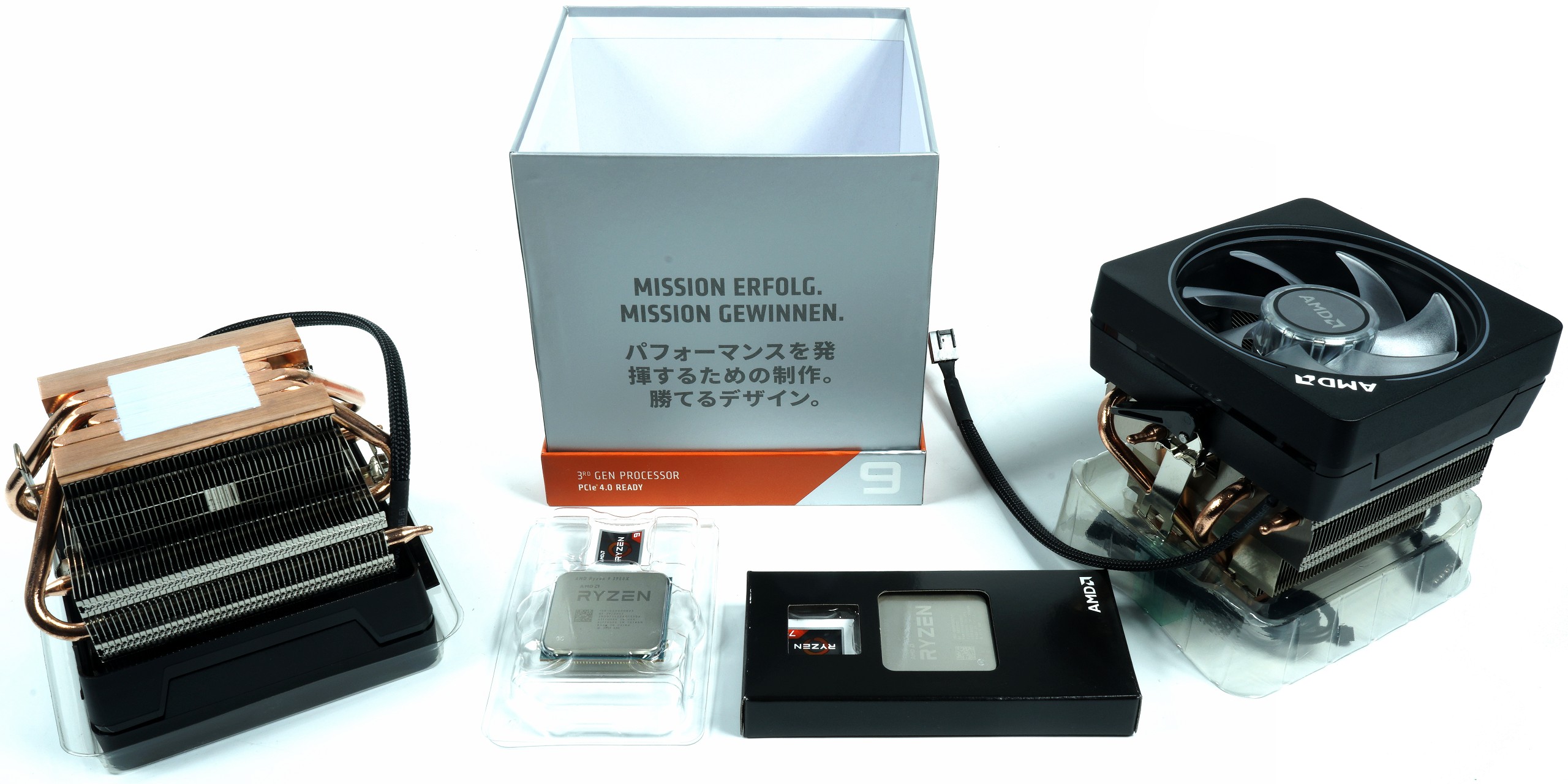
Since there are always questions and some things are often confused, we will give you some insights into AMD-UEFI, what is colloquially called “the BIOS” (although it is no longer correct). I have also broken down the following extremely to remain as simple and understandable as possible. Nevertheless, what happens when the PC starts up is the classic hen-and-egg problem that you simply have to talk about. Software starts hardware, whereas hardware without software does not actually work and software without hardware does nothing. Now what?
The mysterious bootloader and the AGESA
To break this node (hardware doesn’t work without software) you need a boot loader. Also and especially with regard to security, AMD has decided in 2013 to install an additional microprocessor, the so-called PSP (Platform Security Processor). This PSP can be compared quite well with Intel’s Management Engine for CPUs, because in the end it all comes down to the same thing. And where is this mysterious PSP now? You won’t find it on the motherboard, that would be too easy. No, the PSP itself is a simple ARM Cortex processor core, which is directly integrated in the CPU die and continues to run and can be used in the background even after hardware initialization. So in an AMD CPU containing such a PSP, the boot process only starts when the x86 rest is in a paused state and only the PSP is allowed to run. We’ll remember that.
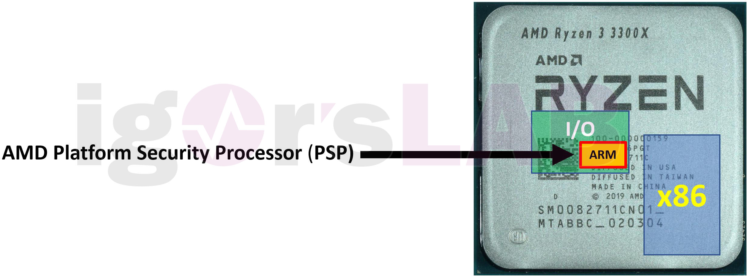
But back to the CPU and the actual boot process. And at this point we already come to the first term that comes up again and again when it comes to AMD CPUs (stability, compatibility, performance), the AGESA, AMDs Generic Encapsulated Software Architecture. We know that the CPU is the first thing that is initialized when the PC is switched on and it contains the so-called On-Chip Bootloader for this very purpose.
The PSP begins execution in its boot ROM (read-only memory programmed at manufacture), which contains simple code that verifies and then loads the off-chip PSP boot loader located in the SPI flash. This AGESA boot loader (ABL) then performs the actual hardware initialization in further steps, but I’ll come back to that in a moment. However, the boot loader first reads and authenticates the first block of BIOS code and only if successful does it release the processor from its paused state. At this point, the x86 processor takes over the execution parallel to the PSP. This is called Hardware Validated Boot, AMD’s extension of Secure Boot, where the PSP acts as the hardware root of trust.
For those who want to know exactly: The boot ROM starts searching for the magic value 0x55AA55AA, which in turn is part of the FIRMWARE_ENTRY_TABLE structure. This structure, also known as ROMSIG, is located at a predefined position within the SPI Flash. This structure tells the boot ROM where the PSP directory is located. The boot ROM then loads a hard-coded decryption key (“chip key”) into the PSP’s cryptographic coprocessor, also known as the CCP. The CCP keeps this key in its key memory block from which it does not allow the key to be read. From this point on, the key may only be used for encryption and decryption operations. The boot ROM firmware then reads and decrypts the now encrypted PSP boot loader from the BIOS image located in the SPI flash and then executes it.
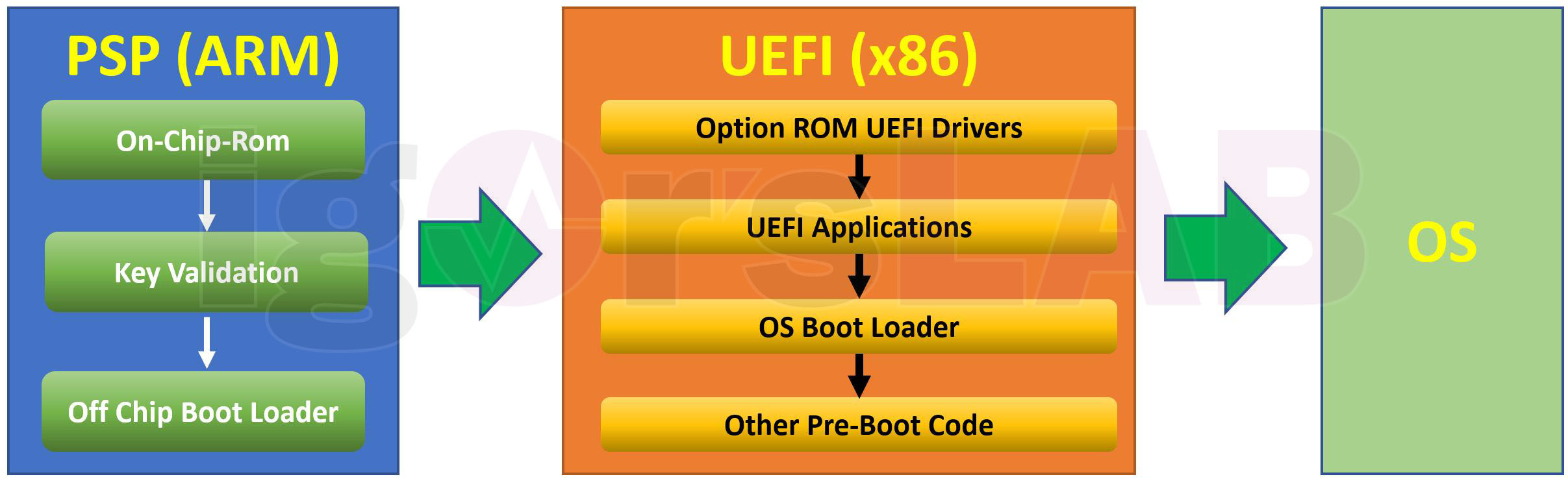
The AGESA boot loader also loads the UEFI image into memory and later, after hardware initialization, passes control to the UEFI, which is still often (almost folkloristically) referred to as “the BIOS”. The AGESA firmware then takes care of the rest of the initialization and booting of the x86 cores and the initialization of the main memory (DDR4 training).
However, since the UEFI cannot possibly have access to all hardware-specific internals and the specification does not provide for overclocking of a processor, it is the task of the respective board partner to extend the UEFI and supply the necessary firmware for addressing the hardware. For this purpose, AMD provides an interface that is also included in the AGESA code (UEFI drivers) and enables developers to change the core voltage of the processor, for example. The firmware required for this and the documentation for the implementation of the whole system is then distributed to UEFI manufacturers such as AMI or Phoenix.
And what exactly is Combo PI?
In the end, the Combo means nothing else than that several SoCs (with own firmware) are supported and the PI stands for Platform Initialization. However, this version should not be lumped together with the AGESA version, because Combo PI is virtually the parent container (ABL, PSP, SMU, VBIOS for APUs, etc.), which also contains the AGESA data. Whereby – it is probably better to think of it as one big folder containing the source code for the drivers and the binaries (firmware) of all SoCs. This is then sent to the BIOS manufacturers and they turn it into the actual UEFI image according to AMD’s specifications. PI without the addition of Combo, but with the SoC name in front of it is also available. These versions work only as Naples PI, Rome PI or for Summit Ridge.
And now you can also safely guess why, for example. a first generation Ryzen is no longer running on many current motherboards: the firmware has simply become too large due to the many entries with tens of processor variants and one had to start reducing the entries again. Besides the commercial intention to sell something new, it also simply fails because of the final size of the file. Of course you can also increase the flash memory, but many customers are already complaining about the long boot times until the post-screen.
That’s exactly why AMD, starting with the new B550 motherboards, has started to slim down the whole thing by restrictively excluding stored products and the microcode required for them, so that the firmware can be loaded faster and with less effort. They leave the back door open for Ryzen 2 and the X570 chipsets, but I would like to bet that the next generation will be the end of bloated and funny.
Interesting here is the supposed number salad, which however follows a fixed pattern. The following diagram from the AMD documents now provides information about the individual positions:

Normally, of course, you will only be offered things where the second and third numbers are both a zero. Anything else would then not be a final status and should, if at all, be enjoyed with the necessary caution. We are done with that and to be honest: it wasn’t that complicated after all, was it?


Kommentieren