


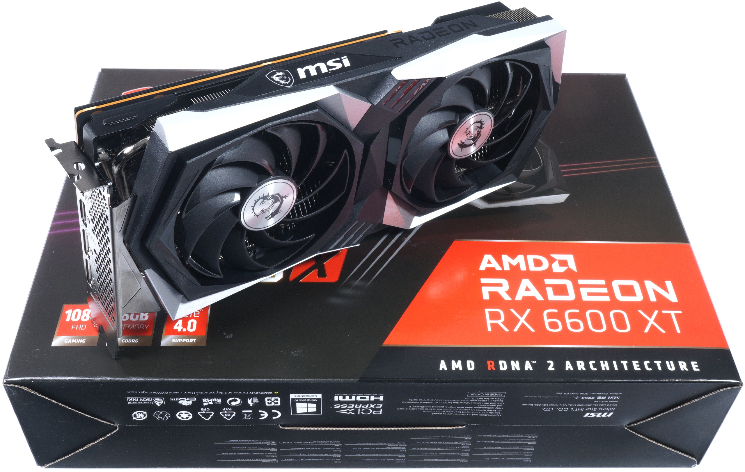
AMD rounds out the Navi portfolio further down the line with the Radeon RX 6600XT unveiled today. Since the reference cards are only available as render picture (AMD is following NVIDIA’s lead here with the GeForce RTX 3060), today’s launch article will use a board partner card. And since I also did the launch of the GeForce RTX 3060 with a Gaming X card from MSI at the time, I’m happy about the card AMD gave me (randomly). Because this also allows a better comparison of the cooling solutions and the factory OC of both cards.
The other board partner cards may not be unveiled until tomorrow, and there are already products in the pipeline for those as well. But more on that at the appropriate time. The Navi23 chip in the RX 6600XT is new and we’ll take a closer look at it in a moment. In general, however, graphics cards are currently a sensitive topic, so that one has to separate very strongly between technical and emotional considerations. Therefore, let’s please leave miners, scalpers and the partly already megalomaniac retail sector aside for now and dedicate ourselves purely to the technology for the time being.
And what about the prices? Since everything can’t be predicted, I have to consult the MSRP in USD here, even though the comparison is of course lame in many respects. AMD is talking about an MSRP of $379 for the basic Radeon RX 6600 XT board partner cards, the MSRP of the NVIDIA GeForce RTX 3060 was $329 at the time, and the GeForce RTX 3060 Ti was $399. This positions AMD a bit closer to the RTX 3060 Ti in terms of price, but I’m still comparing it to both cards and basing it off the GeForce RTX 3060 without Ti because it’s the entry point to the current 1080p class.
The Radeon RX 6600 XT as reference design
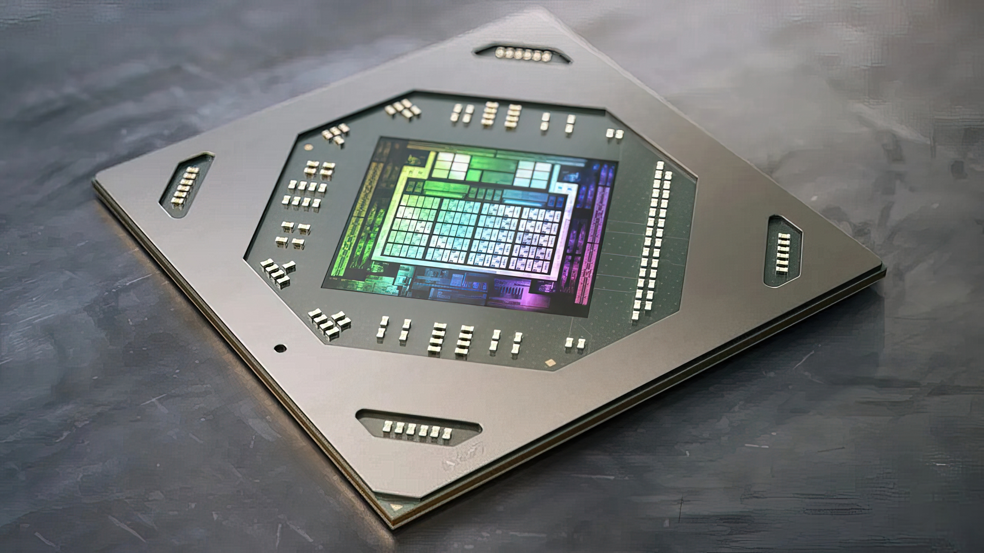
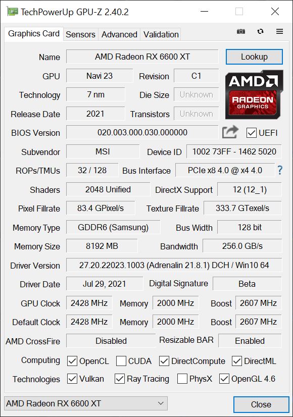
The AMD Radeon RX 6600 XT relies on the Navi 23 XT GPU, which has 32 compute units or 2048 stream processors. The card also features 32MB of Infinity Cache and 8GB of GDDR6 memory running over a 128-bit wide bus interface. The Navi 23 GPU itself measures 237 mm2 and consists of 11.06 billion transistors. However, the GPU is still not the smallest chip in the RDNA 2 family, as Navi 24 is still expected here for the absolute entry-level range. Storage speeds will be at the usual 16 Gbps, which will then give a total bandwidth of 256 GB/s. The MSI Radeon RX 6600 XT Gaming X 8 GB clocks with 2428 MHz and could reach up to 2607 MHz at its peak, which looks decent on paper at first and is even surpassed in practice in some places.
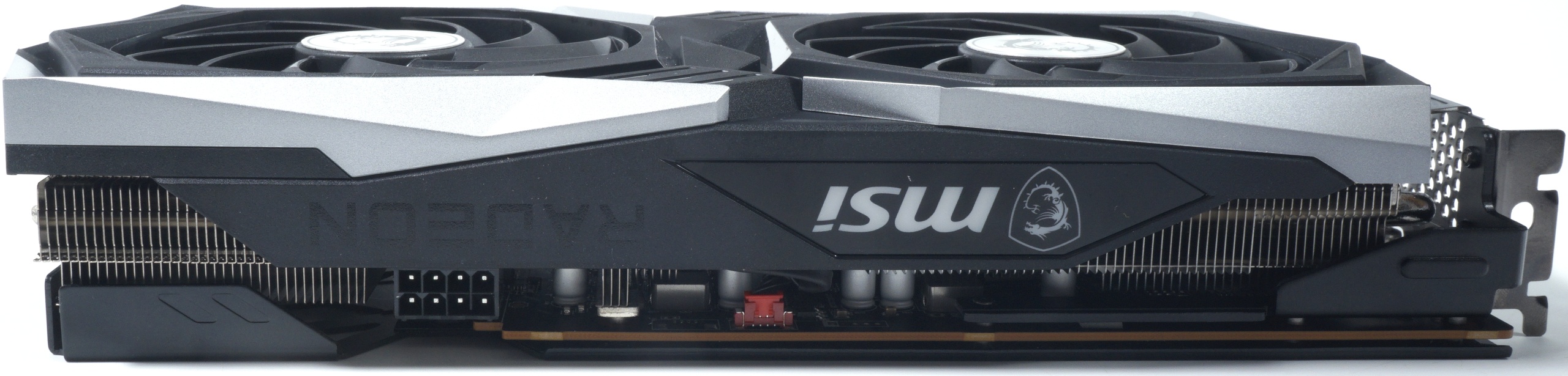
The MSI card weighs only 873 grams and turns out to be a real lightweight here. The front is dominated by two current 9.5 cm fans, whose design we already know from the other MSI cards. The rest is ABS in dark grey and silver along with an RGB illuminated logo on the top. It’s not a real upset, but it’s not a visual aberration either. It’s all right.
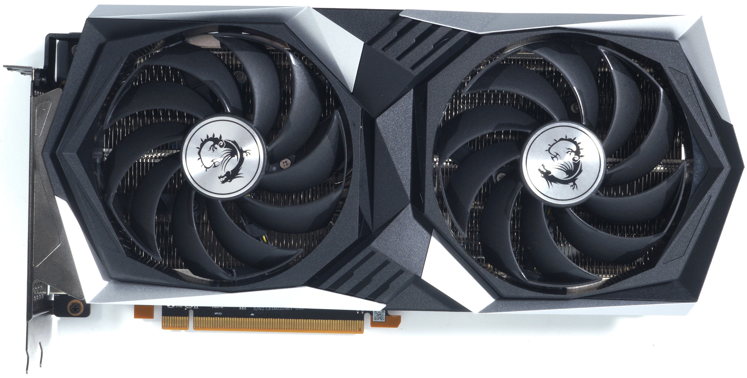
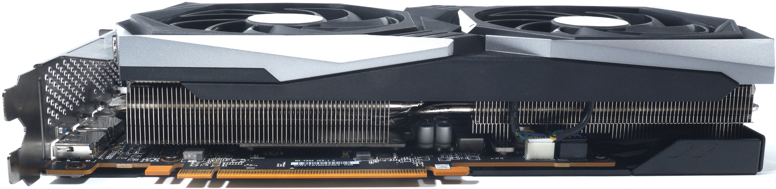
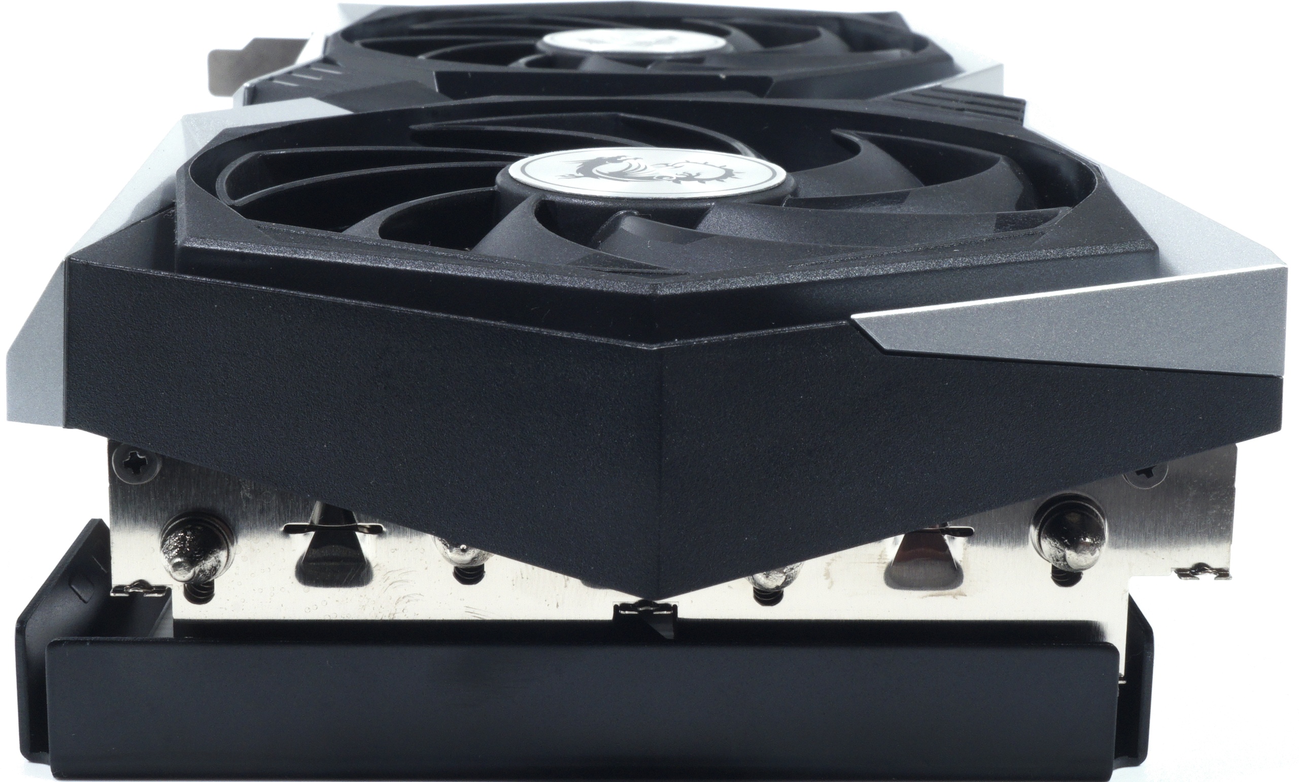


The board is already 4.5 cm thick without the backplate and needs another 0.4 cm for the rear planking. The cooling fins are vertical and on the top we see a single 8-pin power supply connector. The rest, however, is completely unspectacular. The height from the top edge of the motherboard slot is 12.5 cm, which is not exactly low. But you have to accommodate the fans somehow.
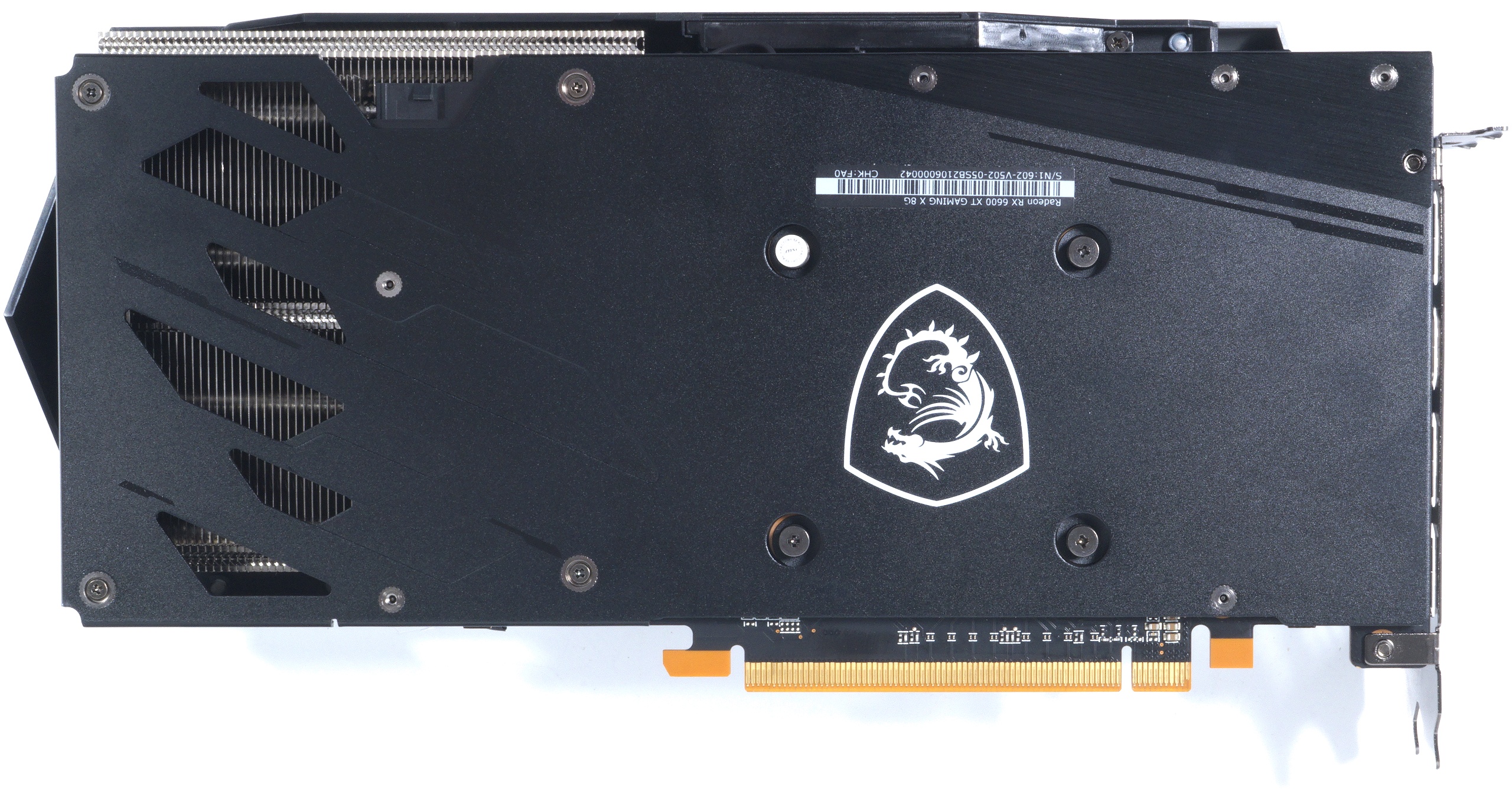
The backside of the board is covered by a backplate. the air opening also reveals that the board with its 25 cm length is quite a bit shorter than the 27.5 cm long card (slot bracket to card end).

The slot bracket is closed, carries 1x HDMI 2.1 and three current DP connectors. The USB Type C is omitted. The whole thing is powered via an 8-pin socket. More about this on the next page in the teardown.
The screenshot from GPU-Z then provides information about the remaining data of the card:
Again, I have a table for all statisticians among you, before it really gets going from the next page on.
| Model | RX 6600 XT (MSI) |
RX 6700 XT | RX 6800 | RX 6800 XT | RX 6900 XT | RX 6900 XT LC |
|---|---|---|---|---|---|---|
| GPU | Navi 23 | Navi 22 | Navi 21 | Navi 21 | Navi 21 | Navi 21 |
| Process node | 7 nm | 7 nm | 7 nm | 7 nm | 7 nm | 7 nm |
| The Size | 237 mm2 | 336 mm2 | 520 mm2 | 520 mm2 | 520 mm2 | 520 mm2 |
| Transistors |
11.06 billion | 17.2 billion | 26.8 billion | 26.8 billion | 26.8 billion | 26.8 billion |
| Compute units | 32 | 40 | 60 | 72 | 80 | 80 |
| Shader | 2048 | 2560 | 3840 | 4608 | 5120 | 5120 |
| TMUs/ROPs | TBA | 160/64 | 240 / 96 | 288 / 128 | 320 / 128 | 320 / 128 |
| Game clock | 2428 MHz | 2424 MHz | 1815 MHz | 2015 MHz | 2015 MHz | 2250 MHz |
| Boost Clock | 2607 MHz | 2581 MHz | 2105 MHz | 2250 MHz | 2250 MHz | 2345 MHz |
| Memory GDDR6 |
8 GB | 12 GB | 16 GB | 16 GB | 16 GB | 16 GB |
| Infinity cache | 32 MB | 96 MB | 128 MB | 128 MB | 128 MB | 128 MB |
| Memory bus | 128-bit | 192-bit | 256-bit | 256-bit | 256-bit | 256-bit |
| Memory clock | 16 Gbps | 16 Gbps | 16 Gbps | 16 Gbps | 16 Gbps | 18 Gbps |
| Bandwidth | 256 GB/s | 384 GB/s | 512 GB/s | 512 GB/s | 512 GB/s | 576 GB/s |
| TDP | 160 W | 230 W | 250 W | 300 W | 300 W | 330 W |

- 1 - Einführung und Testsystem
- 2 - Testsystem und Methodik
- 3 - Teardown, Platinenanalyse und Kühler
- 4 - Gaming Performance Full-HD
- 5 - Gaming Performance WQHD
- 6 - Gaming Performance DXR & FSR vs. DLSS
- 7 - Details: Frames per Second (Curve)
- 8 - Details: Percentiles (Curve)
- 9 - Details: Frame Times (Bar)
- 10 - Details: Frame Times (Curves)
- 11 - Details: Variances (Bar)
- 12 - Leistungsaufnahme und Effizienz der Einzelspiele
- 13 - Leistungsaufnahme: Übersicht & Netzteil-Empfehlung
- 14 - Temperaturen und Infrarot-Tests
- 15 - Geräuschemission / Noise
- 16 - Zusammenfassung. Features und Fazit


40 Antworten
Kommentar
Lade neue Kommentare
Veteran
Moderator
Mitglied
Urgestein
Veteran
1
1
Veteran
Veteran
Veteran
Mitglied
Urgestein
Veteran
Mitglied
Mitglied
Urgestein
Veteran
Urgestein
Mitglied
Alle Kommentare lesen unter igor´sLAB Community →