


Intel’s breakthrough enables continued scaling and promotes Moore’s Law: glass substrates for advanced packaging technologies are coming this decade. Yet Intel’s research and work on this technology goes back a decade. In Chandler, Arizona, Intel has now built a fully integrated glass R&D line with more than $1 billion in investment. Glass substrates enable an order of magnitude improvement in design rules needed for future data center and AI products. They offer huge performance and density increases over organic substrates.
Chip architects can thus fit more “chiplets” in a smaller footprint in a package. Significantly improved mechanical, physical and optical properties allow more transistors for better scaling and assembly of larger chiplet complexes. Complementing this, improved density and power characteristics result in lower overall cost and lower power consumption. Chip architects thus gain greater flexibility in their designs.
Intel’s focus on glass substrates:
- Working closely with equipment and materials partners to enable a homogeneous ecosystem
- Electrically functional, assembled MCP test vehicles with 3 layers of RDL and TGV at 75 µm
- Filled through-glass vias with an aspect ratio of about 20:1 for a core thickness of 1 mm, suitable for AI and data centers
- Over 600 inventions related to architecture, process, equipment and materials
Why Glass versus Organics?
- Higher temperature tolerance offers 50% less pattern distortion
- Glass substrates have ultra-low flatness, enabling improved depth of field for lithography
- Dimensional stability required for extremely tight layer-to-layer interconnect overlays
- Up to 10-fold increase in interconnect density possible with glass
- Improved mechanical properties of glass enable ultra-large form factor packages with very high assembly yields
- Glass offers improved flexibility in establishing design rules for power supply and signal routing
- Ability to seamlessly integrate optical interconnects as well as embed inductors and capacitors into the glass during higher temperature processing operations
- Better power supply solutions while achieving high-speed signal transmission required at much lower power.
The slides below provide more details and visuals on glass substrates:
Glass Core Substrates
Intel’s assembly and test technology development fabs in Chandler, Arizona, in July 2023
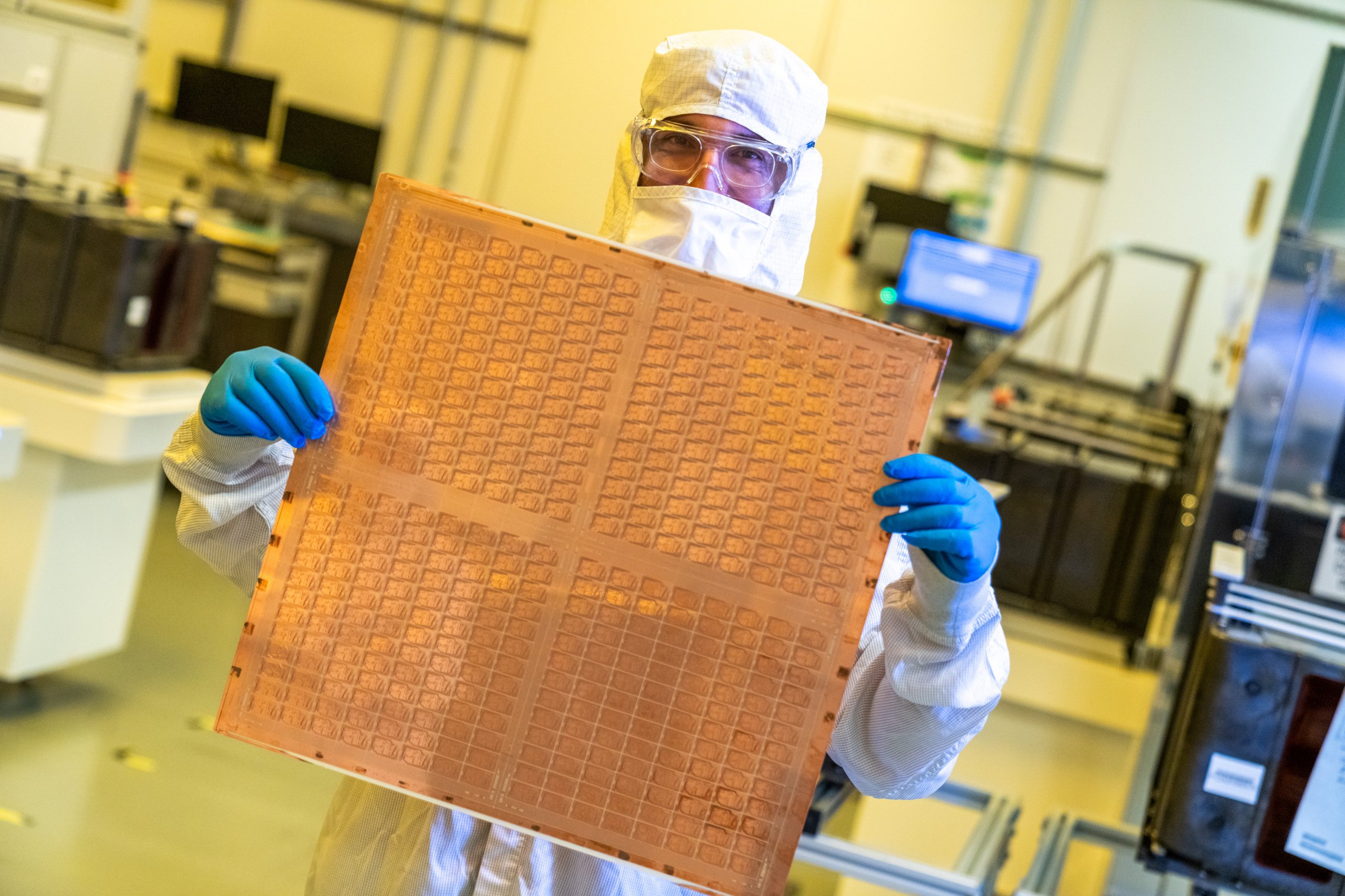
Intel’s advanced packaging technologies are realized at the company’s assembly and test technology development fabs. A short photo gallery once again shows a few impressions of the new manufacturing facility. In the first picture, one of Intel’s engineers holds a test glass core substrate panel in the camera.
The next photo shows glass-substrate test units at Intel’s assembly and test technology development fabs in Chandler, Arizona, in July 2023
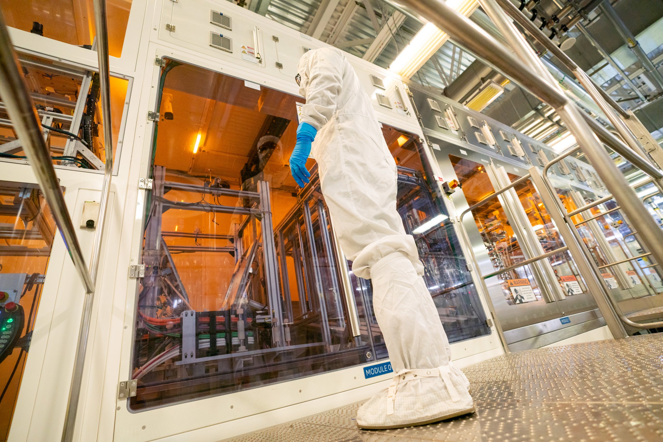
An Intel engineer works on a tool to remove lithography resist from glass-core substrates.
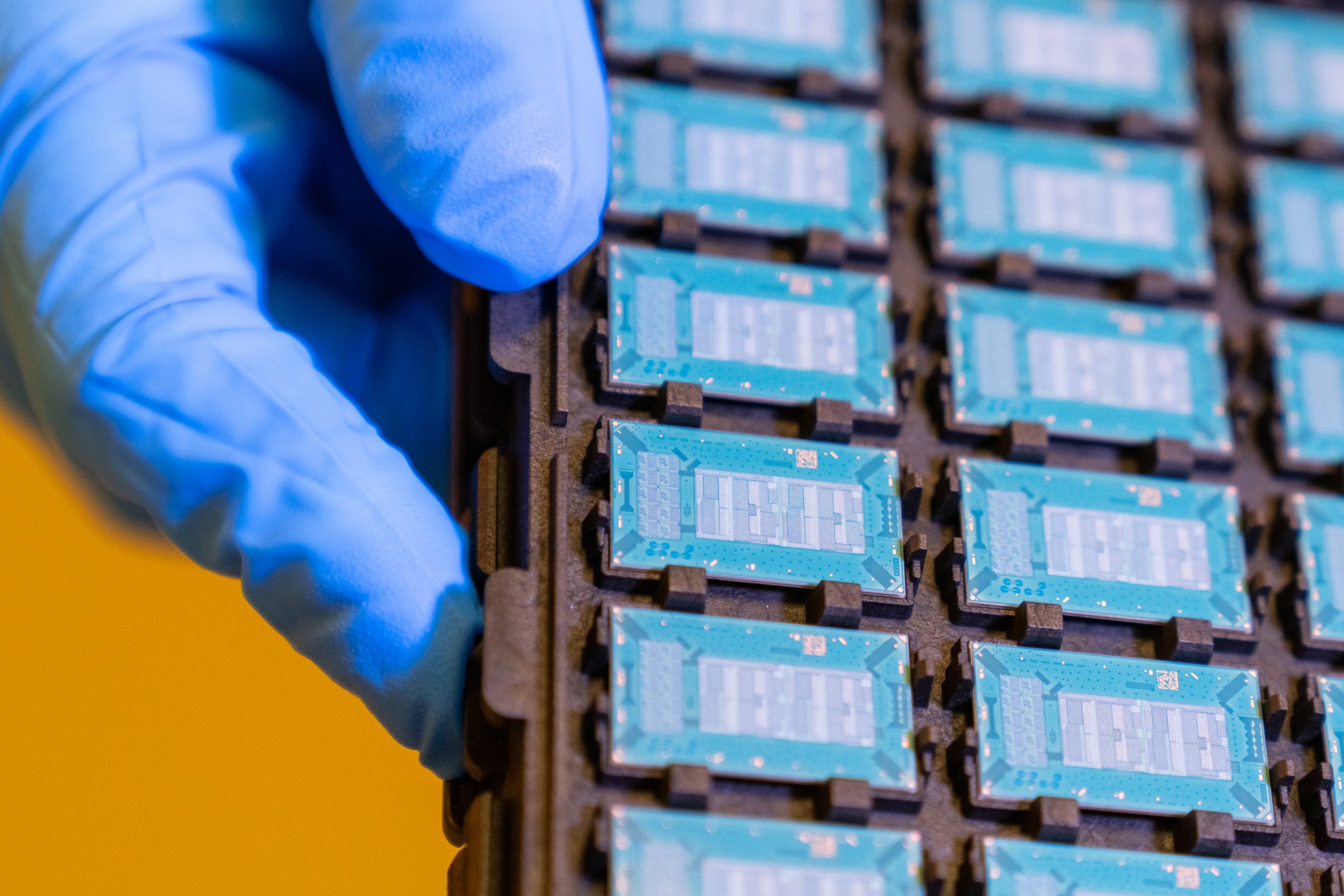
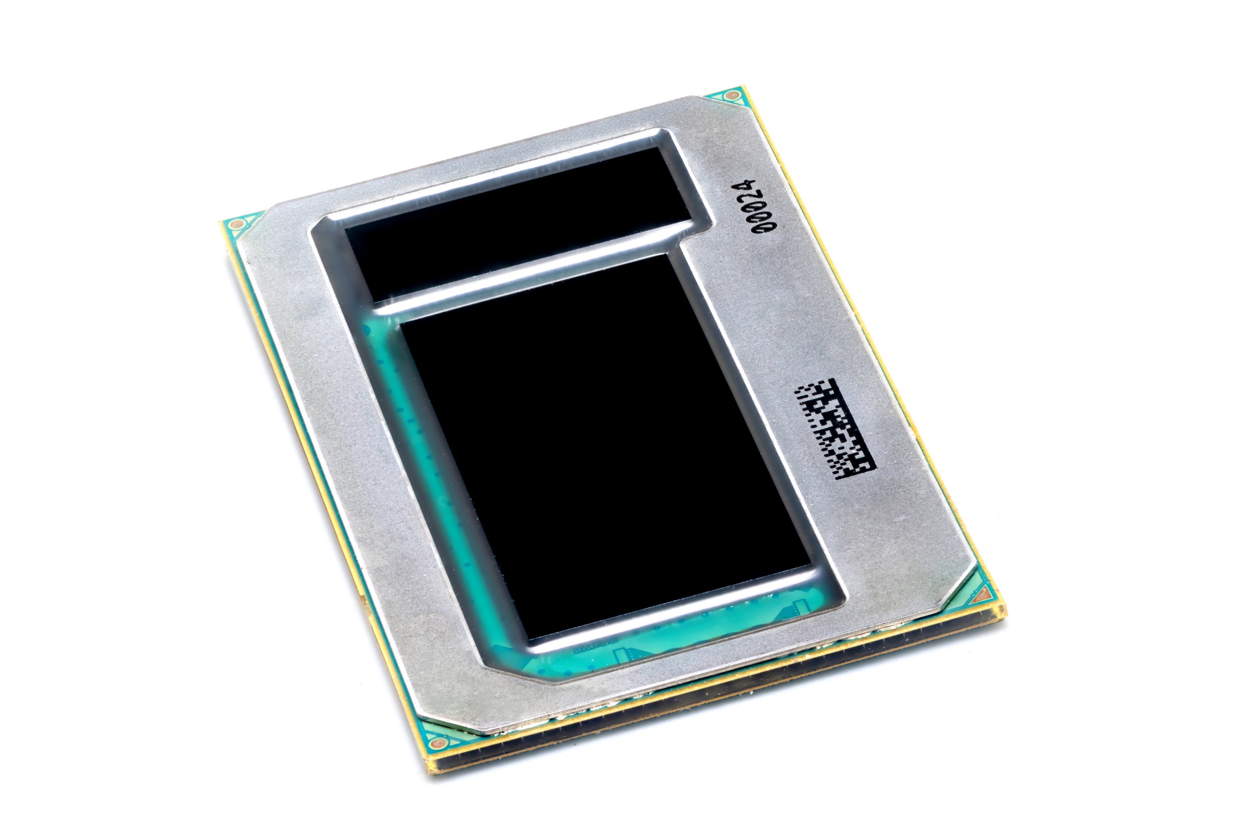
The next photo shows the ball grid array side of a glass-substrate test chip assembled by Intel….
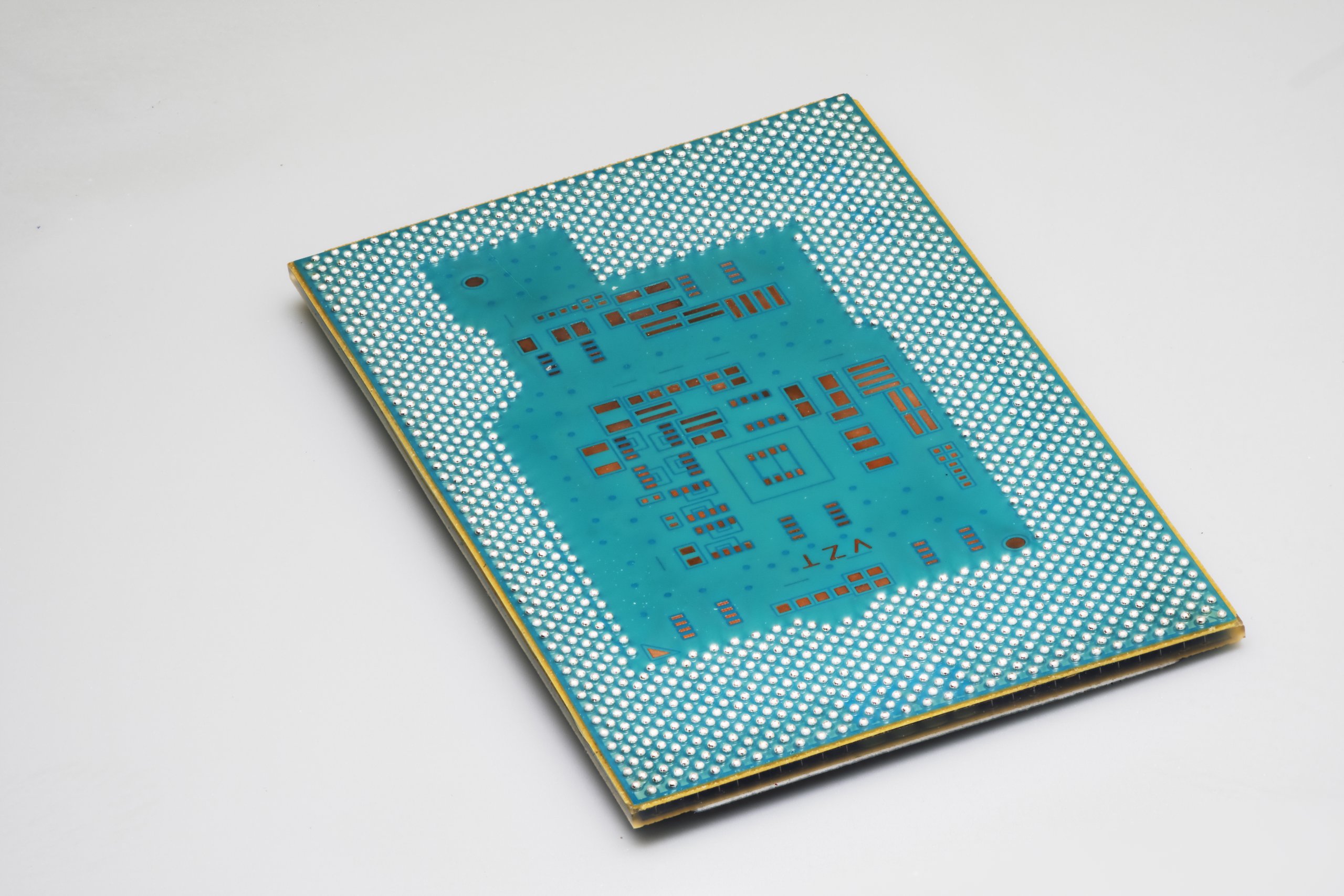
…and the next the multi-die assembly side of a glass-substrate test chip assembled by Intel.
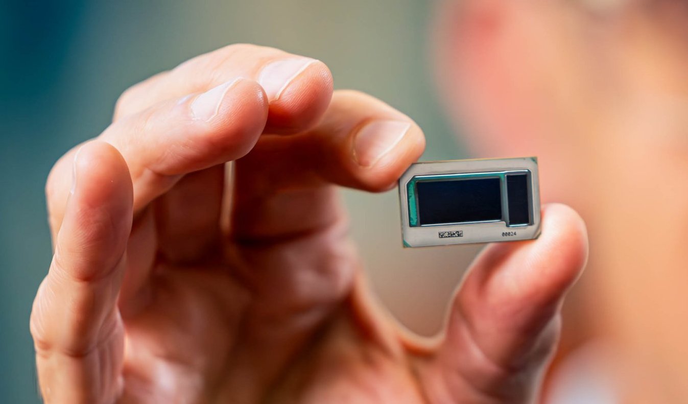
Hamid Azimi, corporate vice president and director of substrate technology development at Intel Corporation, holds up a glass substrate test chip assembled by Intel to the camera.

The text and image materials were provided by Intel under BDA. The condition was to meet the embargo deadline of 3 p.m. on September 18, 2023.


6 Antworten
Kommentar
Lade neue Kommentare
Urgestein
Veteran
Urgestein
1
Urgestein
Urgestein
Alle Kommentare lesen unter igor´sLAB Community →