Reasons for the post-test
In our Pascal Roundup: GeForce GTX 1070 and GeForce GTX 1080 we reported in great detail about the EVGA GeForce GTX 1080 FTW and the cooling problems we identified. At the beginning of September, we had already informed EVGA about the thermal problem zones identified and passed on our measurement data to the manufacturer. In the meantime, EVGA has responded and largely followed our recommendations for a modification.
On its website, EVGA now offers a so-called thermal mod, which consists of an optional, free set of thermal guide pads and a suitable BIOS for the affected cards – because it meets a whole range of models that match a similar cooler without active cooling of the voltage transformer components.
If you don't trust yourself, EVGA also offers an assembly service, as you can easily see from the homepage.
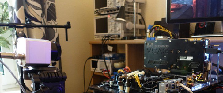
Now that the pads have been available in Europe since this week, we want to take a close look at this mod. We have deliberately waited so long to be able to measure with the original pads, because this is essential for a fair and objective evaluation.
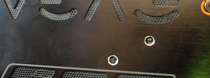
In order to remain as practical as possible, we drilled two holes into the backplate at the two hottest points of our first test and also omitted the pads below in a circular manner in order to be able to measure directly on the board with our infrared camera. Since it is the same map as from the first test, the results are also directly comparable.
We use our standard test system, as we described in detail in our Roundup. The conditions for a direct comparison are therefore met.
Additional memory gate or not?
Various images that have now appeared in forums also show that the pads used at the factory between the front panel and the memory modules should not completely fill the existing distance. We recreated the test with several EVGA GeForce GTX 1080 FTW or have other users do so. In all cases, however, the following picture emerged, with no column visible:

This means in these cases that the pads are properly installed at first, but also with us there were no very deep traces of impression. On the images that appear on the Internet, the pads all stick to the front plate and the gap is located below between the memory module and the pad. This, in turn, is quite remarkable, because in order to understand the whole thing correctly, one should also know how such a graphics card is made.
In the Manual Insertion Line, the pads are almost exclusively glued to the memory modules, the front panel only later comes onto the card together with the backplate. But if a pad sticks to the plate, it must have had a firmer contact at least once before!
After removing the backplate, if you remove the additional screws of the front plate, which are initially obscured by the backplate, the front plate stands out slightly obliquely and very similar, rather oblique gaps are created. This also applies if you screw the backplate back on, but have simply forgotten the few additional screws during assembly.
Column, however, could occur with the GeForce GTX 1070 with this cooler type if the GDDR5 memory modules have a height difference to the GDDRX5 modules and/or the DDR5-Samsung or DDR5-Samsung. -Micron modules also vary in highs – tolerances are always available. And since the pads on the memory modules were kept as thin as possible, (here the subjunctive is important to us) such behavior could occur.
However, since all these aspects have been rather speculative at the moment, we do not want and cannot make a final judgment here. However, we will stick to it and, if necessary, will continue to report.
Updated on Nov 14, 2016, 10:00 a.m.
EVGA has just told us that the memory pads will also be made 0.2mm thicker to be 100% safe. This applies both to the pads that are supplied with the thermal mod that is being applied, and to the mass production itself, which is now being changed.
In any case, the BIOS is now flashed ex works, but EVGA has also assured us that the old, quieter BIOS will continue to be offered as an optional download. In the end, you have the choice of where the preferences lie.
Multi-layer boards and durability recommendations
In our measurements, we have paid more attention to the temperature load of individual components, but have always completely hidden the board material. On this point, too, however, we need to make some critical comments – especially if it is partly permanently above 100°C. That's why we got smart again at the R&D of a graphics card manufacturer.
The board uses a glass fibre composite material, which is a derivative of the material commonly referred to as FR4 with epoxy resin matrix, but has been enriched with mineral fillers in such a way that a lower thermal expansion of the printed circuit board during heating can be guaranteed and you also remain RoHS compliant.
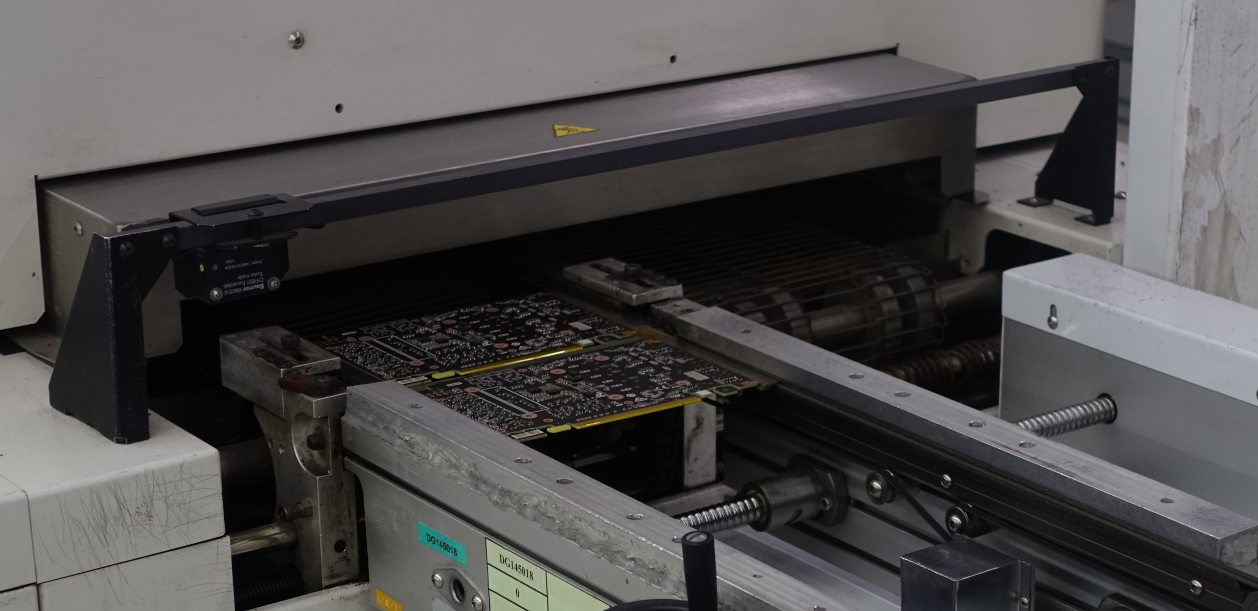 After reflow soldering (example)
This is primarily used to guarantee increased safety during the production process, especially when soldering the final soldering in the shaft soldering bath. However, since these are only short-term loads, the elasticity and thus the expansion of the resin mixture does not increase to such an extent that possible demolitions on the internal traces or even delaminations can occur on the boards.
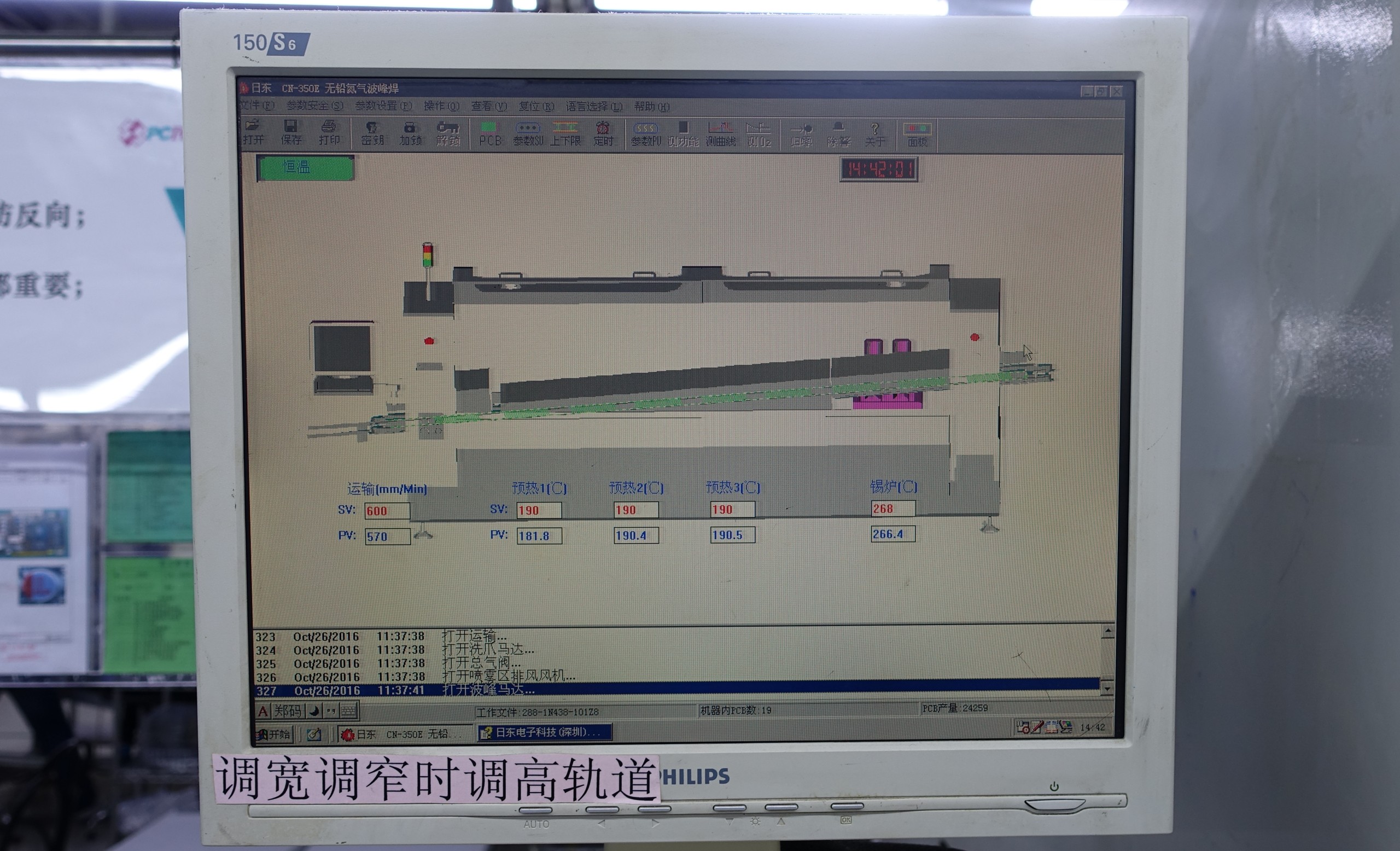 Temperatures at wave soldering bath (example)
Unfortunately, this improvement of the material for the production processes does not affect the maximum permissible continuous operating temperature!
This continuous operating temperature depends on the epoxy resin matrix used and should not exceed a maximum of 95 to 100° recommended for FR4 boards, so that the material can be outgassed/dried out or at least delayed. The consequences of these irreversible material changes are also demolitions, delamination and even bending.
The EVGA mod with the thermal guide pads
EVGA now offers a fairly easy-to-run mod to help adequately mitigate the hotspots that occur. Since we are curious which pad has what influence, we will do the tests in three steps: first only with the pad between the back of the board and the backplate, then with this pad and another pad between the front plate and the cooling fins of the cooler, and this all again together with the BIOS flash.
We also want to answer the often asked question whether the BIOS flash with the disadvantages of a much louder card will really be necessary and whether one could even do without it under certain conditions.
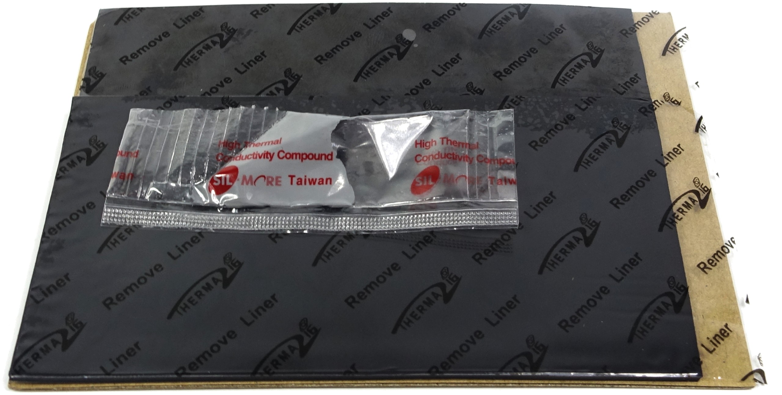
EVGA delivers a larger (back) and a smaller thermal pad (front) in a plastic bag and completes the whole with original EVGA thermal paste. This is needed later when it comes to preparing the cooler for the mod on the front plate. The backplate, on the other hand, is very easy to remove.
EVGA recommends attaching the larger of the two pads as shown below. However, it is also located in some places on a protective film, with which EVGA has closed most of the holes in the backplate. We have left it in its original condition, but would recommend that we remove these thermally unfavourable covers better in order to gain even more contact surface and also improve ventilation.
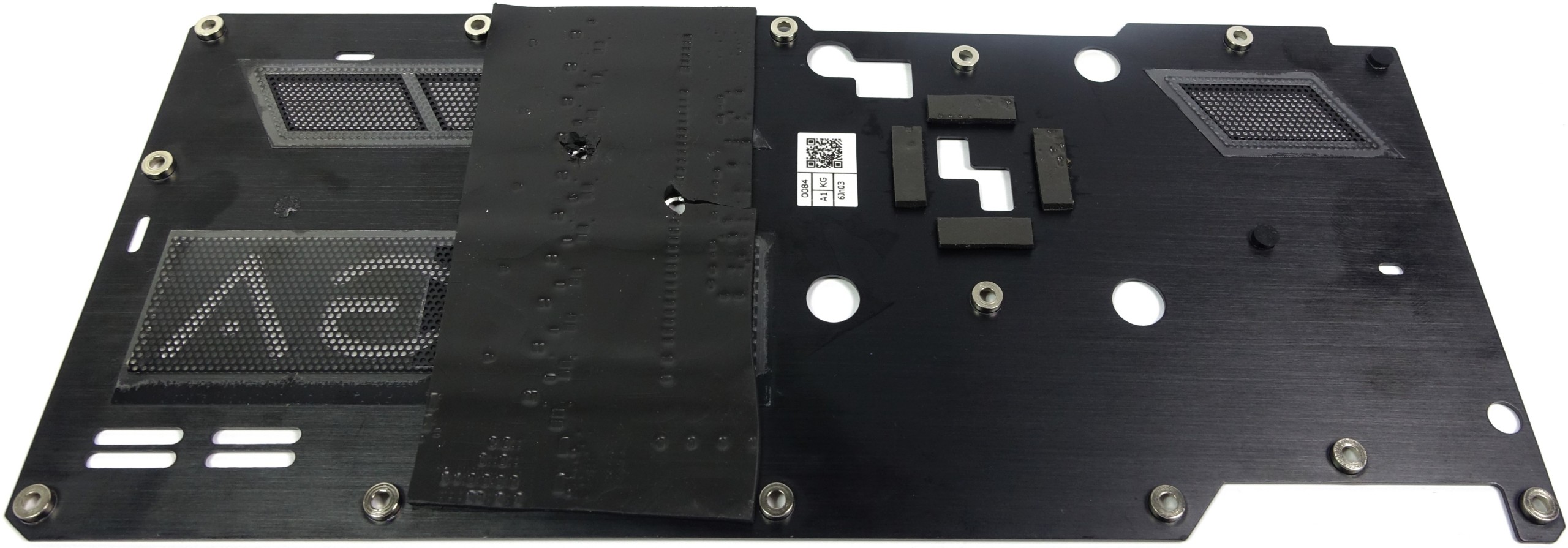
Using the darker surface on the PCB, we can see where the pad was placed during assembly. Since this becomes visible over a large area, one can assume a very good contact of the relatively sticky pad, which also belongs qualitatively to the better variety. The component connectors have also left some visible imprints in the pad.
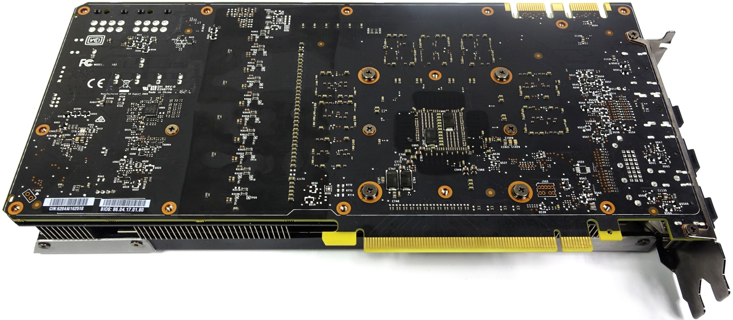
We see that the voltage converter ranges are completely covered and the RAM is at least partially covered. If you want to optimize the whole thing a little bit, put the pad about two centimeters further to the right (seen from the back of the board!) and cut rectangular recesses at the top and bottom of the right edges for later screwing, so that the pad does not make these holes Covered.
The sticking of the front plate is somewhat tricky, because EVGA explicitly recommends covering the long-hole recess for the coils and thus creating a closed surface, which is also high enough to be sufficient with the cooling fins of the main cooler. make contact.
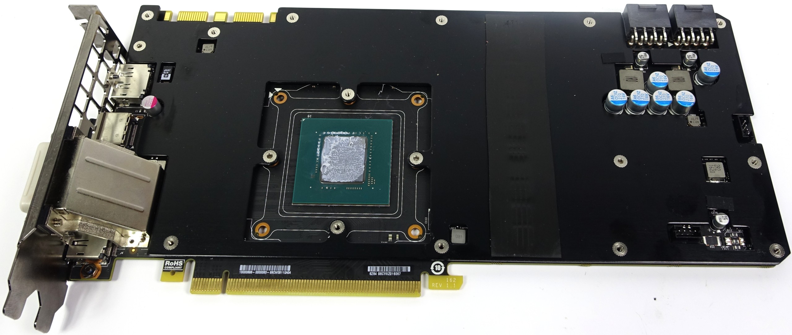
The recording after the reassembly shows us the imprints in the places as more or less clearly recognizable stripes where this contact took place. Here, the area of the coils was cooled, which on your part was one of the hottest candidates of the first measurements. This should also make it possible to significantly reduce the heat distribution on the board in its propagation towards memory and GPU.

The results of the measurements on the next page will show us how well this existence has succeeded in the end (or not).





Kommentieren