


Before I act as a (future) painter and create a possible package including the dimensions known so far, we should review the rumors and leaks of the last days. Let’s take the usually well-informed Kopite7kimi at the word leak, who mentioned a tape-out of the GA102 chip on Samsung and not TSMC on Twitter. This means that a launch as early as 2020 is more than likely, especially since various activities were already taking place in the background, which also affected the respective board partners. The Base-Design-Kit for the boards and the Thermal Design Guide for the boards with the GA 102 are said to have already been distributed diligently.
“NO TEU. GA102 has taped out. It was based on SAMSUNG 10nm. And the new tegra will use the same process node
If this time it should be Samsung instead of TSMC, Nvidia might have gambled a little too heavily with TSMC when it came to the price negotiations for the 7 nm production (the GA102) and Samsung was used as an argument for a possible price reduction. Or else Nvidia generally views the whole thing from an economic point of view and initially uses the much cheaper 8 nm node from Samsung, which is actually an improved 10 nm node. Thus, there would still be a full node jump between what Samsung offers and what was previously manufactured at TSMC in 12 nm for Nvidia.
Considering the economics, an even larger chip in Samsung’s 8 nm node is unlikely to make much economic sense anyway. This makes all the data on the GA102 and the other branches that have been circulated so far sound plausible. I would also like to point out once again that the nodes cannot really be compared with each other. Samsung’s 8 nm node is actually closer to the 10 nm than to the 7 nm, especially since the fin pitch between 10 and 8 nm remains comparable and only the gate pitch has been reduced by 6 percent.
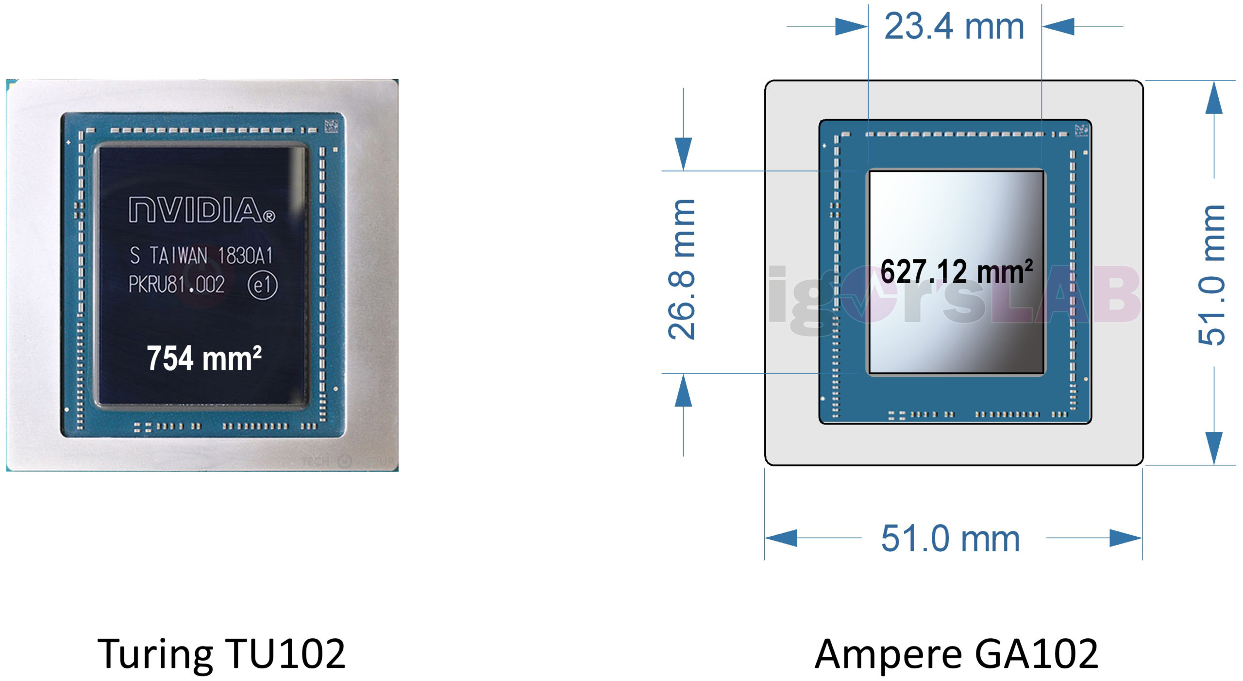
The possible package as graphic
And now my small, highly speculative work of art comes into play, which is based on circulated dimensions and is quite in line with my extrapolation at the time. If the latest information is correct, the edge lengths of the chip would result in a chip area of 627.12 mm². Assuming that the process of Samsung compared to the old node, the same number of transistors to about 40% of the area, then the extrapolation already made of approx. 6000 to 6100 shaders for the full expansion with this chip size quite realistic. Of course, the number of shaders also refers to their complexity, and nobody can yet say what the ratio of CUDA to RT and especially Tensor cores will be.
Separate power supply should come
I had already speculated that from a more efficient operation point of view it would be necessary to decouple the power supply of the CUDA cores from the RT and Tensor cores externally and not to solve this in the GPU via different paths. This would create additional space and increase efficiency. With NVDD and MSVDD (“miscellaneous”), even this small problem would then be elegantly solved. Especially since the share of MSVDD is supposed to be much higher than that of VDDCI for AMD cards. And what about the already extrapolated 230 watts, which should be delivered to the GPU?
I think that 60 to 70 watts is the minimum that can be used for the additional arithmetic-logic units in the GA102 full configuration, and if the whole thing is decoupled from the CUDA cores, then the power supply can be made a little simpler there as well. In a previous calculation I had used 16 voltage converter circuits for pure GPU power at 230 watts. In addition, up to 4 additional control loops would be required for the memory, at least with a full 24 GB configuration.
Of course, you can use the calculator and data sheet to make an estimate of how the possible distribution of the GPU voltages could look like. With a bit of imagination (and luck in guessing), you could set the supply of the shaders with up to 10 phases, whereby each phase would then only address one power stage. The remaining up to 6 phases were then allocated to another partial voltage with the same power stage distribution.
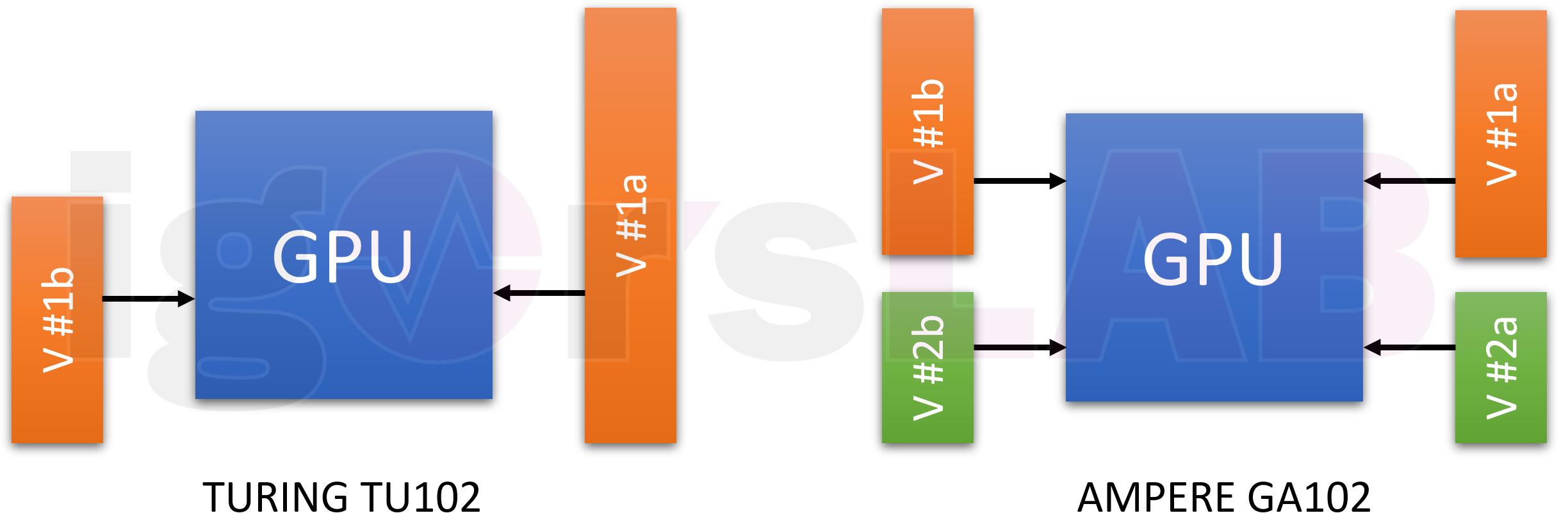
If you calculate this further, the shaders would only have a maximum of 160 to 170 watts, which would make the ratio between Turing and ampere more realistic again. In the case of notebooks, for example, Dynamic Boost is used, where the power distribution is shifted as required in order to remain within the thermal and power limits. A smart balancing between the possible two partial voltages, where the tensor and RT cores would be weighted at least equally, would actually be only logical.
That should be it for today, because we do not want to speculate so much. Just a little. But at least a grain of salt will probably be on it, as always, which then also tastes a little like truth. Let’s hope so 🙂
Source: own


Kommentieren