


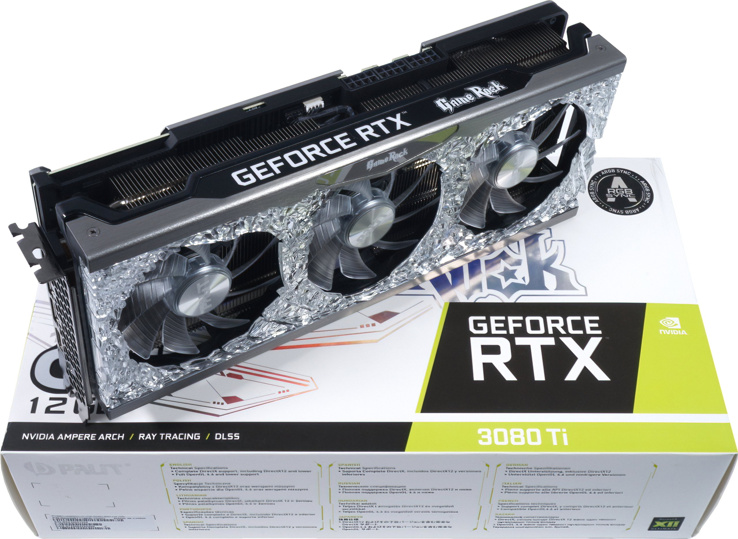
Palit goes its own way with the new Palit RTX 3080 Ti GameRock 12GB in terms of looks. Whether the RGB disco lighting on the front, which is based on an ice shell (crystal design), is really to everyone’s liking, remains to be seen. But it’s a very eye-catching design that polarizes. That in itself is a right to exist. The only restriction for my review: Since there are only a few rotating samples and I also want to leave the original card to the other colleagues, the teardown unfortunately has to be omitted for this card as well. That’s a shame, for sure, but an important part of the deal to get this card.
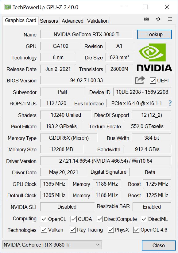
This graphics card has the usual GeForce feature set of the current Ampere generation. The heart of the GeForce RTX 3080 Ti is the GA102-225 graphics processor. It is based on Samsung’s 8nm process node developed specifically for NVIDIA and has a total of 28 billion transistors. We already know him from last year. It measures just under 628 mm², making it the second largest gaming GPU ever produced just below the Turing TU102 GPU.
For the GeForce RTX 3080 Ti, NVIDIA has after all enabled 80 SM units on its flagship, resulting in a total of 10240 CUDA cores. In addition to CUDA cores, NVIDIA’s GeForce RTX 3080 Ti is also equipped with next-generation RT (ray tracing) cores, Tensor cores, and the new SM or streaming multiprocessing units. As for memory, the GeForce RTX 3080 Ti is equipped with 12GB of GDDR6X memory that can deliver memory speeds of 19.0Gbps. Together with a 384-bit interface, this will deliver a cumulative bandwidth of 912.4 Gbps.
Optics and haptics
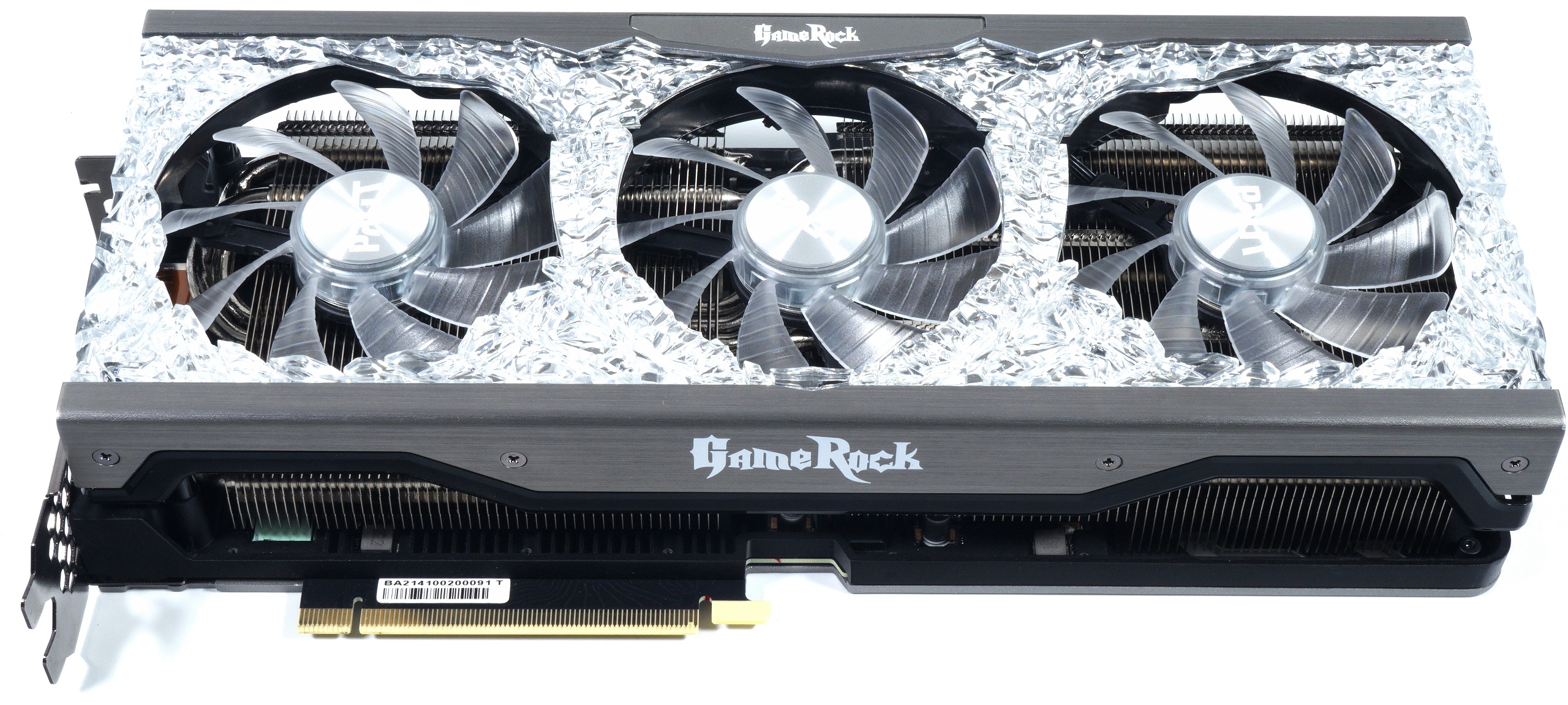
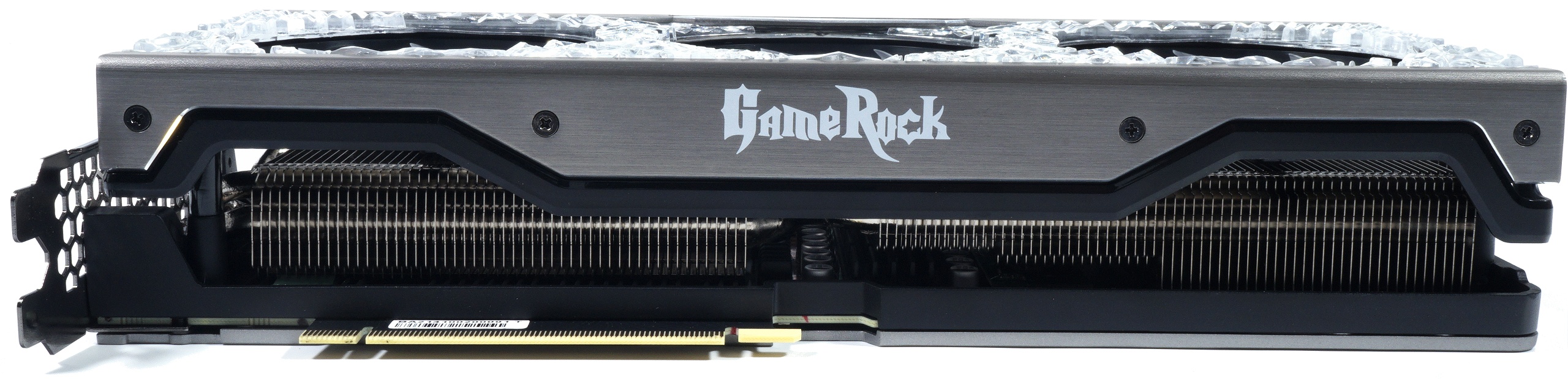
We’ve already been through the formal language. The light metal cover looks good, but you really have to like the one with the icy plastic planking complete with RGB stadium lighting. The Palit RTX 3080 Ti GameRock 12GB weighs 1552 grams and is thus significantly heavier than the reference card. It is also longer with its full 30 cm, stately 12.5 cm high (installation height from PEG) and in addition 5.5 cm thick (2.5 slot design), whereby a backplate and the PCB with altogether five additional millimeters are added.
What looks like a small switch for a dual BIOS on the top is actually a switch for a performance and a silent BIOS. I will only test the performance BIOS today, but will point out the differences in the relevant places. That would clear that up, because the differences are not that extreme. I prefer it cooler and faster.
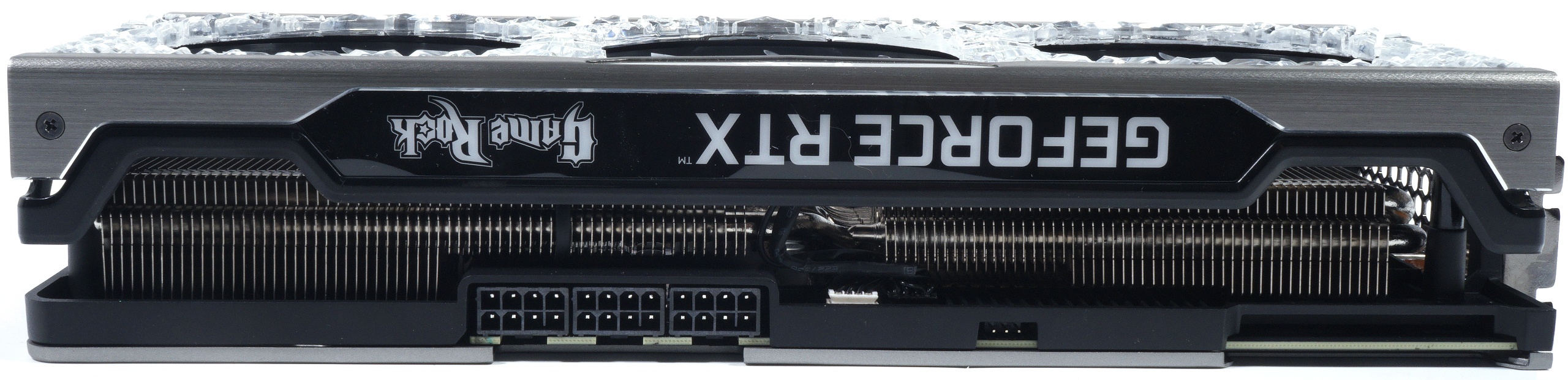
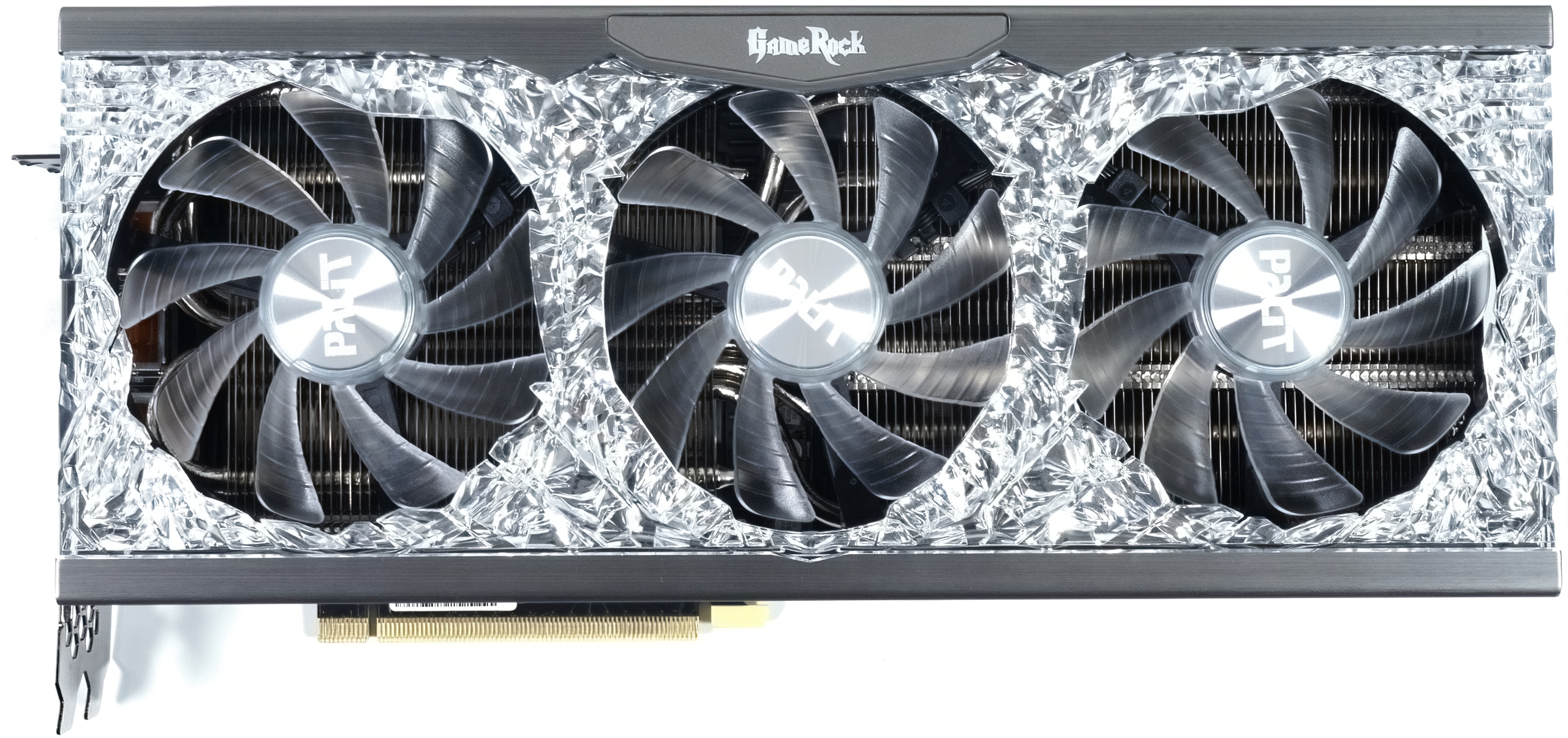
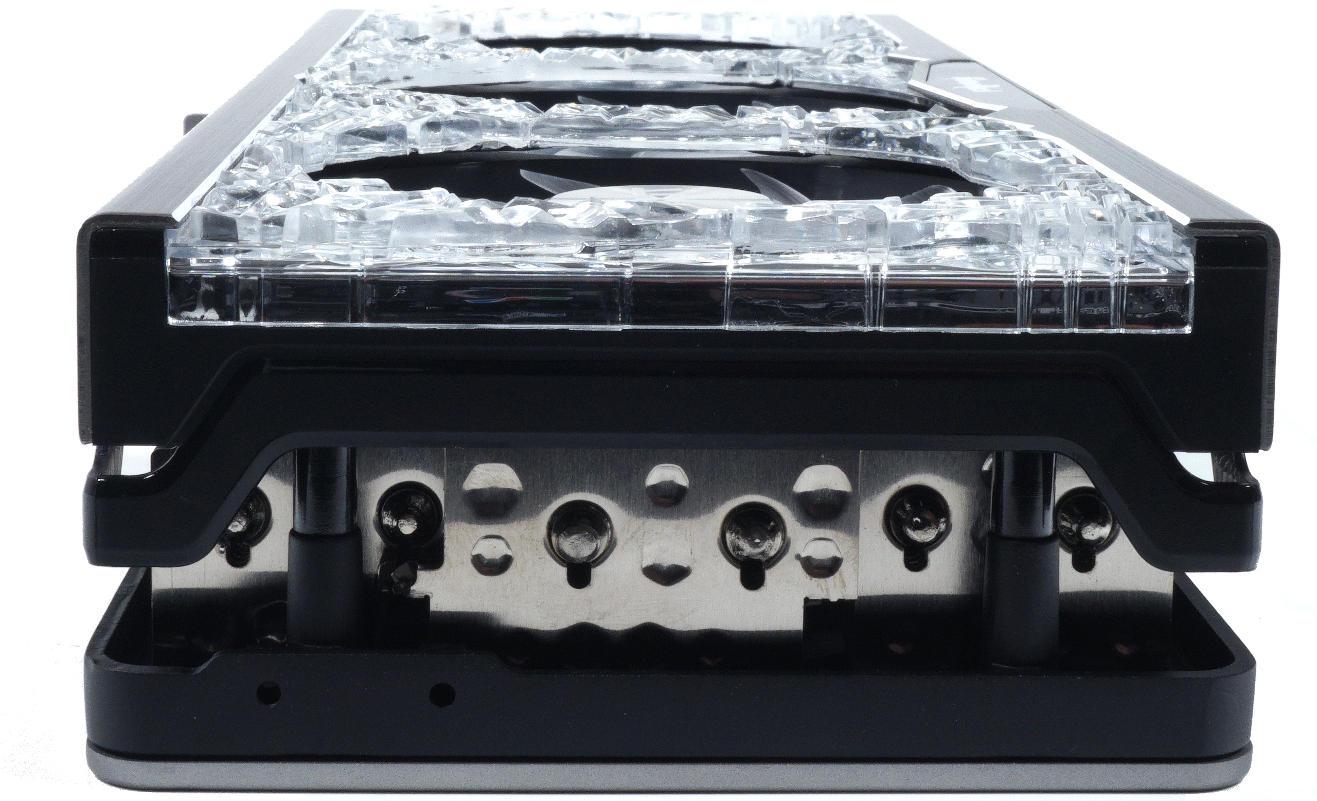
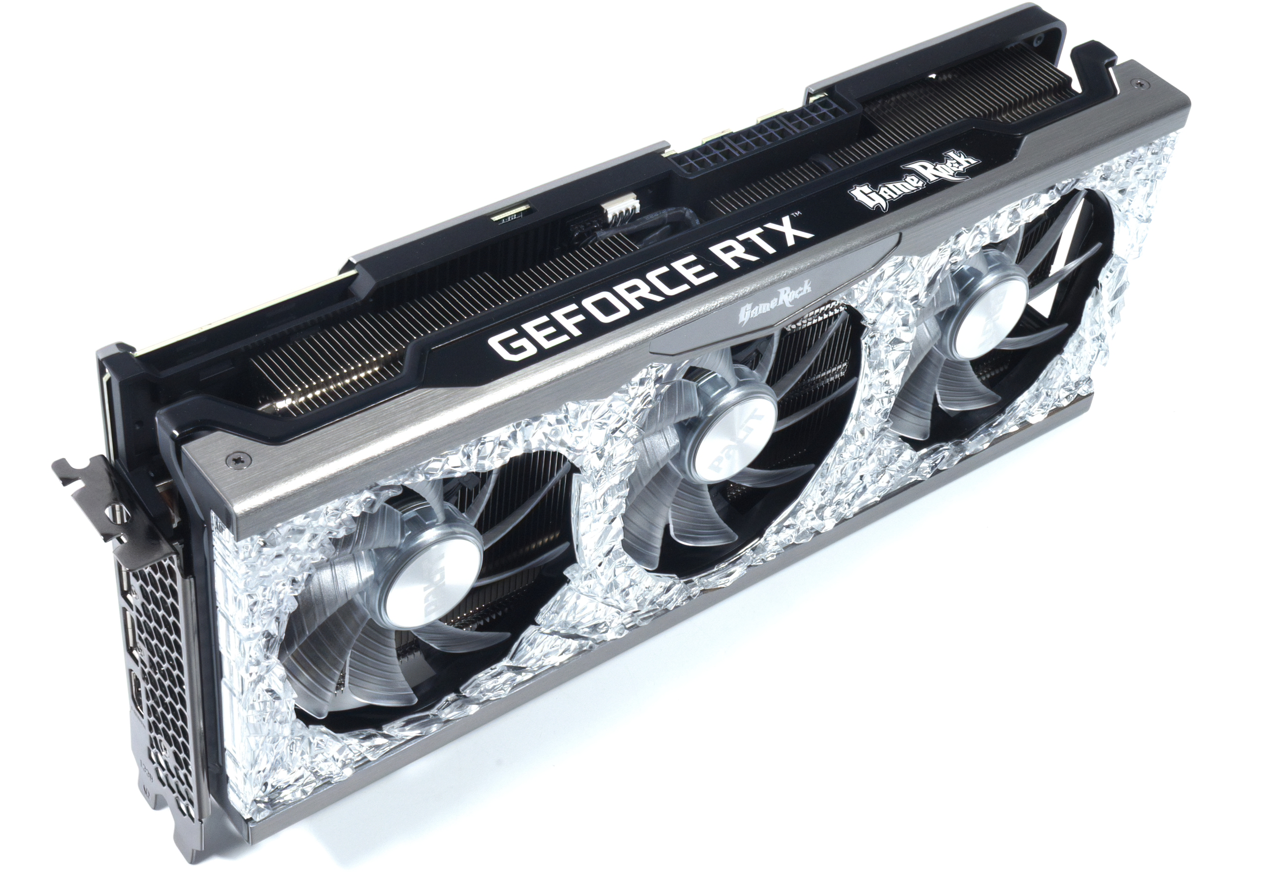
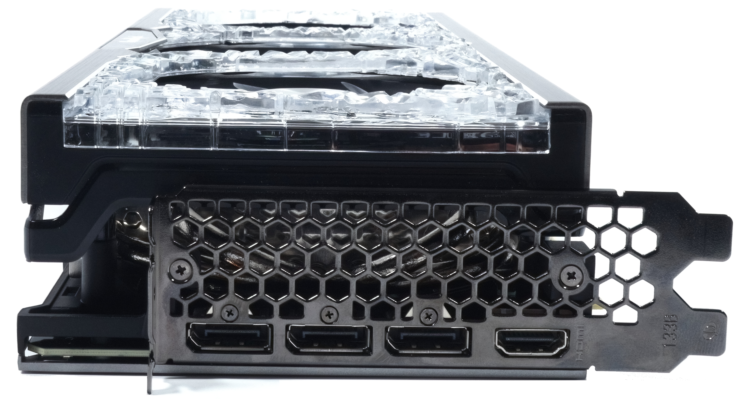
The graphic brick including illumination is supplied via three standard 8-pin sockets, so everything is as known and used, if a card has 400 watts (optionally up to 440 watts) power limit. We also see here the vertical orientation of the cooling fins and the board reinforcement in the form of a backplate and frame. Three 9 cm fans provide the necessary fresh wind for cooling, but the very irregularly shaped openings of the plastic ice shield don’t make sense aerodynamically, rather the opposite. But we’ll get to that later.

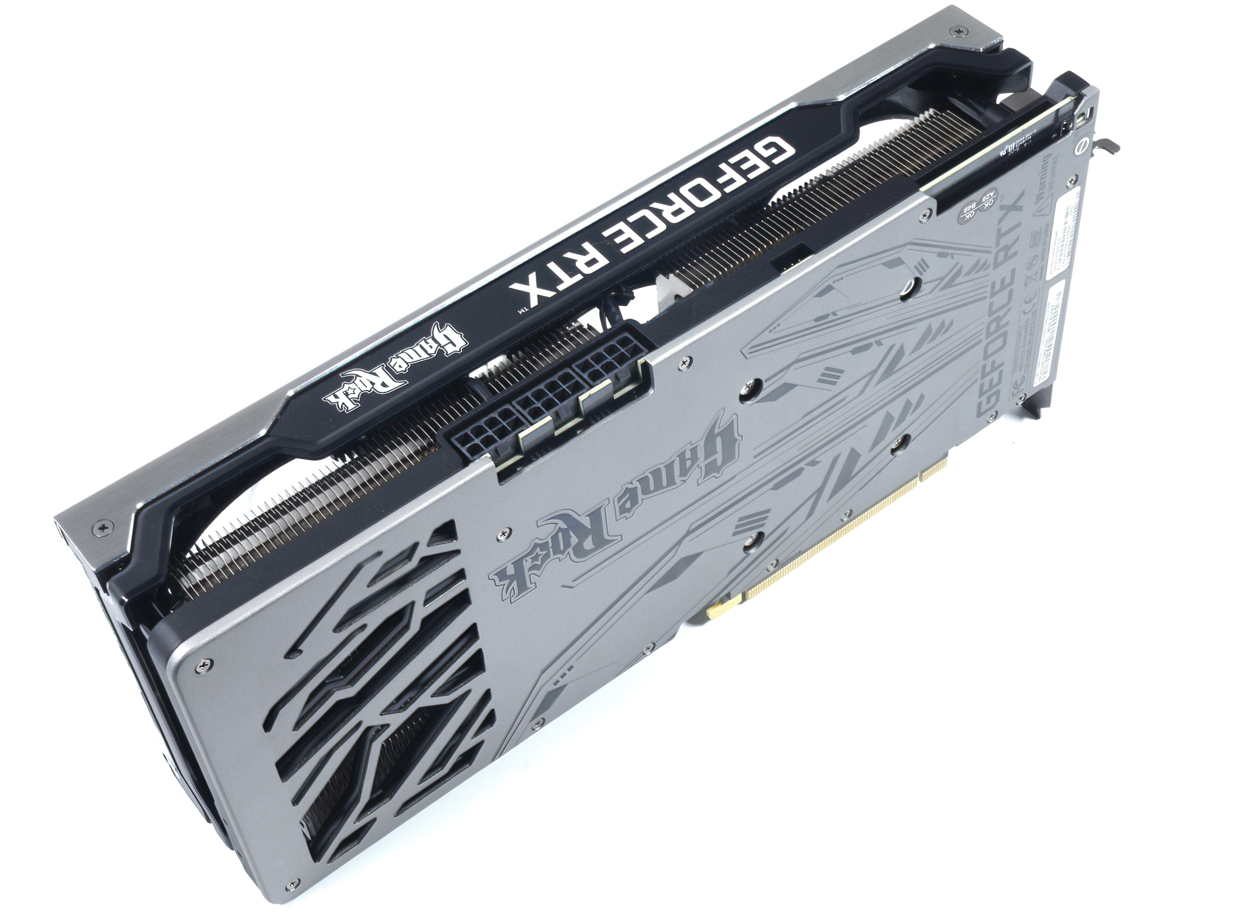

The slot bracket is honeycomb perforated, carries 1x HDMI 2.1 and three current DP 1.4 connectors. The USB Type C port, on the other hand, is missing. More about the construction, the cooler and the assembly I have to owe you this time, because the disassembly was unfortunately taboo. But you can see what works here (or not).
Technology
While the base clock is specified with 1365 MHz, the boost clock is 1725 MHz (FE at 1665 MHz), which is even reached. The card relies on 12GB of GDDR6X at 19Gbps, but we’ve been over that. For the rest of the key data, please refer to the GPU-Z screenshot…
… and the tabular overview (where the values of NVIDIA’s RTX 3080 Ti FE were put in brackets).
| GeForce RTX 3070 | GeForce RTX 3080 | GeForce RTX 3080 Ti |
GeForce RTX 3090 | |
|---|---|---|---|---|
| GPU | GA104-300 | GA102-200 | GA102-225 |
GA102-300 |
| Process node | Samsung 8 nm | |||
| The Size | 395.2 mm2 | 628.4 mm2 | ||
| Transistors | 17.4 billion | 28 billion | ||
| CUDA Cores | 5888 | 8704 | 10496 | |
| TMUs/ROPs | TBA | 272 / 96 | 320/112 |
TBA |
| Tensor/RT | 184 / 46 | 272 / 68 | 320 / 80 | 328 / 82 |
| Base clock |
1500 MHz | 1440 MHz | 1365 MHz |
1400 MHz |
| Boost clock |
1730 MHz | 1710 MHz | 1725 (1665) MHz |
1700 MHz |
| Memory | 8 GDDR6 | 10 GB GDDR6X | 12 GB GDDR6X | 24 GB GDDR6X |
| Interface | 256-bit | 320-bit | 384-bit | 384-bit |
| Throughput | 14 Gbps | 19 Gbps | 19 Gbps |
19.5 Gbps |
| Bandwidth | 448 Gbps | 760 Gbps | 912.4 Gbps |
936 Gbps |
| TGP | 220W | 320W | 400 (350) W |
350W |
| Launch | 15.10.2020 | 17.09.2020 | 02.06.2021 |
24.09.2020 |

- 1 - Einführung und technische Details
- 2 - Testsystem und Methodik
- 3 - Gaming Performance
- 4 - Effizienz und Leistungsaufnahme beim Gaming
- 5 - Leistungsaufnahme, Spannungen und Normeinhaltung
- 6 - Lastspitzen und Netzteil-Empfehlung
- 7 - Taktraten und Temperaturen
- 8 - Lüfter und Geräuschemission ('Lautstärke')
- 9 - Übersicht, Zusammenfassung und Fazit


31 Antworten
Kommentar
Lade neue Kommentare
Urgestein
Urgestein
Mitglied
1
Urgestein
1
Urgestein
Moderator
Veteran
Neuling
Urgestein
Neuling
Urgestein
Urgestein
Urgestein
Urgestein
Urgestein
Urgestein
Urgestein
Alle Kommentare lesen unter igor´sLAB Community →